Metallic bonding structure for copper and solder

a technology of metal bonding structure and solder, which is applied in the manufacture of printed circuits, printed circuit aspects, basic electric elements, etc., can solve the problems of brittleness, large volume of electronic components packaged by wire-bonding or tab technology, and long time-consuming wire-bonding process, so as to promote the yield, quality and service life of electronic products.

Inactive Publication Date: 2010-09-30
NATIONAL TSING HUA UNIVERSITY
View PDF1 Cites 0 Cited by
  • Summary
  • Abstract
  • Description
  • Claims
  • Application Information

AI Technical Summary

Benefits of technology

[0011]Based on the abovementioned technical scheme, the present invention has improvements over the conventional technology. The present invention can reduce the intermetallic compounds (such as Cu6Sn5 and/or Cu3Sn) appearing in the interface where the solder members contact the copper-based members and inhibit the formation of voids. The present invention can prevent the copper-based members from bei

Problems solved by technology

The wire-bonding process has a bottleneck of consuming a longer time.
Further, the electronic component packaged by the wire-bonding or TAB technology has a larger volume, which conflicts the trend of slim and lightweight electronic products.
However, the intermetallic material is an ionic-bond compound, which is usually brittle.
Therefore, over amount of

Method used


Image

  • Metallic bonding structure for copper and solder
  • Metallic bonding structure for copper and solder
  • Metallic bonding structure for copper and solder

Examples


embodiments

[0024]Below, the technical contents of the present invention are described in detail with the embodiments. However, it should be understood that the embodiments are only to exemplify the present invention but not to limit the scope of the present invention.

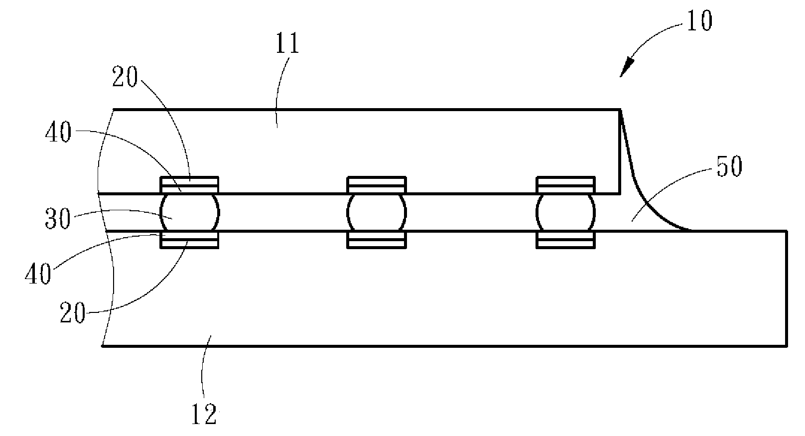
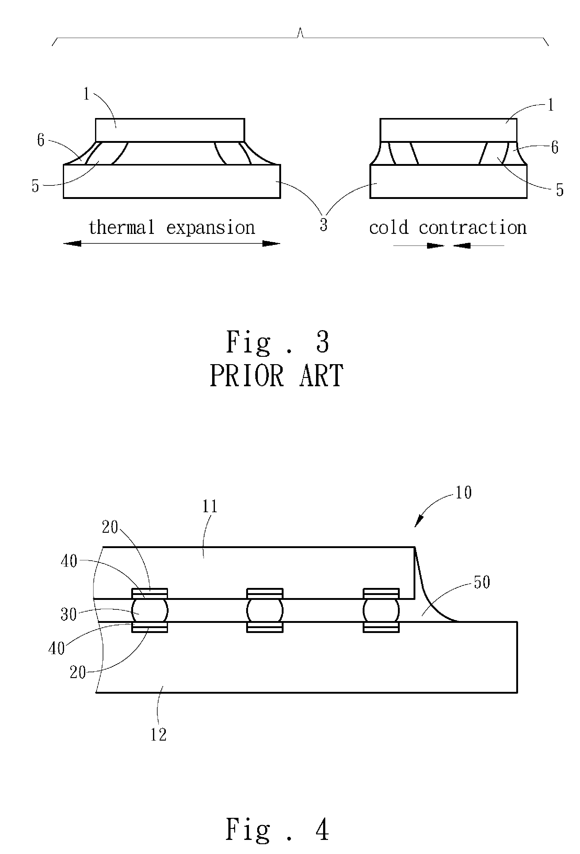
[0025]Refer to FIG. 4 a diagram schematically showing a metallic bonding structure for copper and solder according to the present invention. The present invention proposes a metallic bonding structure for copper and solder, which comprises at least one copper-based member 20 and at least one zinc bonding member 40. The copper-based members 20 are arranged on an electronic element 10. At least one solder member 30 is used to solder the electronic element 10, and the zinc bonding members 40 are arranged between the copper-based members 20 and the solder members 30. The solder members 30 are tin-based solder bumps. The electronic element 10 is a chip 11 or a substrate 12. The zinc bonding member 40 is in form of a film, a sheet, a po...


PUM


Abstract

The present invention discloses a metallic bonding structure for copper and solder, which applies to connect at least one electronic element. The metallic bonding structure comprises at least one copper-based member and at least one zinc bonding member. The copper-based members are arranged on the electronic element through at least one solder member. The zinc bonding members are arranged between the copper-based members and the solder members. The solder members are tin-based solder bumps.

Description

FIELD OF THE INVENTION[0001]The present invention relates to a technology for promoting the strength and reliability of electronic elements, particularly to a metallic bonding structure for copper and solder.BACKGROUND OF THE INVENTION[0002]The first stage of electronic package is to bond a chip to a carrier board via one of the following three technologies-wire-bonding, TAP (Tape Automatic Bonding), and F / C (Flip Chip).[0003]The wire-bonding process has a bottleneck of consuming a longer time. Further, the electronic component packaged by the wire-bonding or TAB technology has a larger volume, which conflicts the trend of slim and lightweight electronic products. Thus, the F / C technology is developed to reduce the size of electronic products.[0004]The F / C technology can achieve a compact, high-pin-count, better-heat-dissipation electronic package. Further, compared with the wire-bonding technology, the F / C technology can greatly reduce the length of the connection wires and effecti...

Claims


Application Information

Patent Timeline
IPC IPC(8): H01L23/488H05K1/02
CPCH01L23/49816H01L2224/48847H01L24/13H01L24/16H01L2224/0401H01L2224/05647H01L2224/13111H01L2224/16225H01L2224/45147H01L2224/73204H01L2924/01029H01L2924/0103H01L2924/0105H01L2924/01078H01L2924/01327H01L2924/014H05K3/244H05K3/3436H05K2201/10674H01L24/05H01L2224/32225H01L2924/15311H01L2224/04042H01L2924/01006H01L2924/01033H01L2924/00014H01L2924/00H01L2924/00012H01L2924/351
Inventor DUH, JENQ-GONGYU, CHI-YANG
Owner NATIONAL TSING HUA UNIVERSITY
Why Eureka
Try Eureka