Array substrate for fringe field switching mode liquid crystal display device and method for fabricating the same

a fringe field switching and liquid crystal display technology, applied in non-linear optics, instruments, optics, etc., can solve problems such as interference between data lines and pixel electrodes, insufficient viewing angle characteristics, and ct or horizontal lines, so as to reduce the area of drain contact holes, reduce ct and horizontal lines, and increase aperture ratio

Active Publication Date: 2013-05-23
LG DISPLAY CO LTD
View PDF6 Cites 32 Cited by
  • Summary
  • Abstract
  • Description
  • Claims
  • Application Information

AI Technical Summary

Benefits of technology

[0033]According to an array substrate for a fringe field switching (FFS) mode liquid crystal display device and a method for fabricating the same in accordance with the present invention, a drain contact hole in the related art that has been formed to electrically connect a drain electrode to a pixel electrode is removed, and an opening portion for exposing an upper portion of the thin-film transistor is formed on an organic insulating layer such that the exposed thin-film transistor and the pixel electrode are electrically connected to each other in a direct manner, and thus an area that has been used to form a drain contact hole in the related art can be used for an opening area, thereby enhancing the transmittance compared to the related art.
[0034]Furthermore, according to an array substrate for a fringe field switching (FFS) mode liquid crystal display device and a method for fabricating the same in accordance with the present invention, a contact hole through which the drain electrode and pixel electrode are electrically connected to each other is formed within the opening portion provided at an upper portion of the thin-film transistor, and thus an area of the drain contact hole can be reduced, thereby increasing the aperture ratio.
[0035]As a result, it has a structure in which the pixel electrode is disposed at the uppermost portion, thereby reducing CT and horizontal line due to capacitance between the data line and pixel electrode.
[0036]Furthermore, according to an array substrate for a fringe field switching (FFS) mode liquid crystal display device and a method for fabricating the same in accordance with the present invention, an amorphous silicon layer (n+ or p+) and an amorphous silicon layer (a-Si:H) containing foreign substances below a conductive layer portion corresponding to the source electrode and drain electrode and the data line are simultaneously patterned, thereby removing a trouble of causing an active tail.

Problems solved by technology

However, the driving of liquid crystals by an electric field applied in the vertical direction has a drawback of providing insufficient viewing angle characteristics.
Furthermore, it has a structure with no contact hole as well as a structure in which the common electrode is disposed at the uppermost portion, thereby causing a problem such as CT or horizontal line due to interference between data pixels.
Accordingly, in case of a structure in which the common electrode is disposed at the uppermost portion, it has a structure in which the pixel is located adjacent to the data line, thereby causing interference between the data line and pixel electrode.

Method used


Image

  • Array substrate for fringe field switching mode liquid crystal display device and method for fabricating the same
  • Array substrate for fringe field switching mode liquid crystal display device and method for fabricating the same
  • Array substrate for fringe field switching mode liquid crystal display device and method for fabricating the same

Examples


Embodiment Construction

[0045]Hereinafter, an array substrate for a fringe field switching (FFS) mode liquid crystal display device and method for fabricating the same according to a preferred embodiment of the present invention will be described in detail with reference to the accompanying drawings.

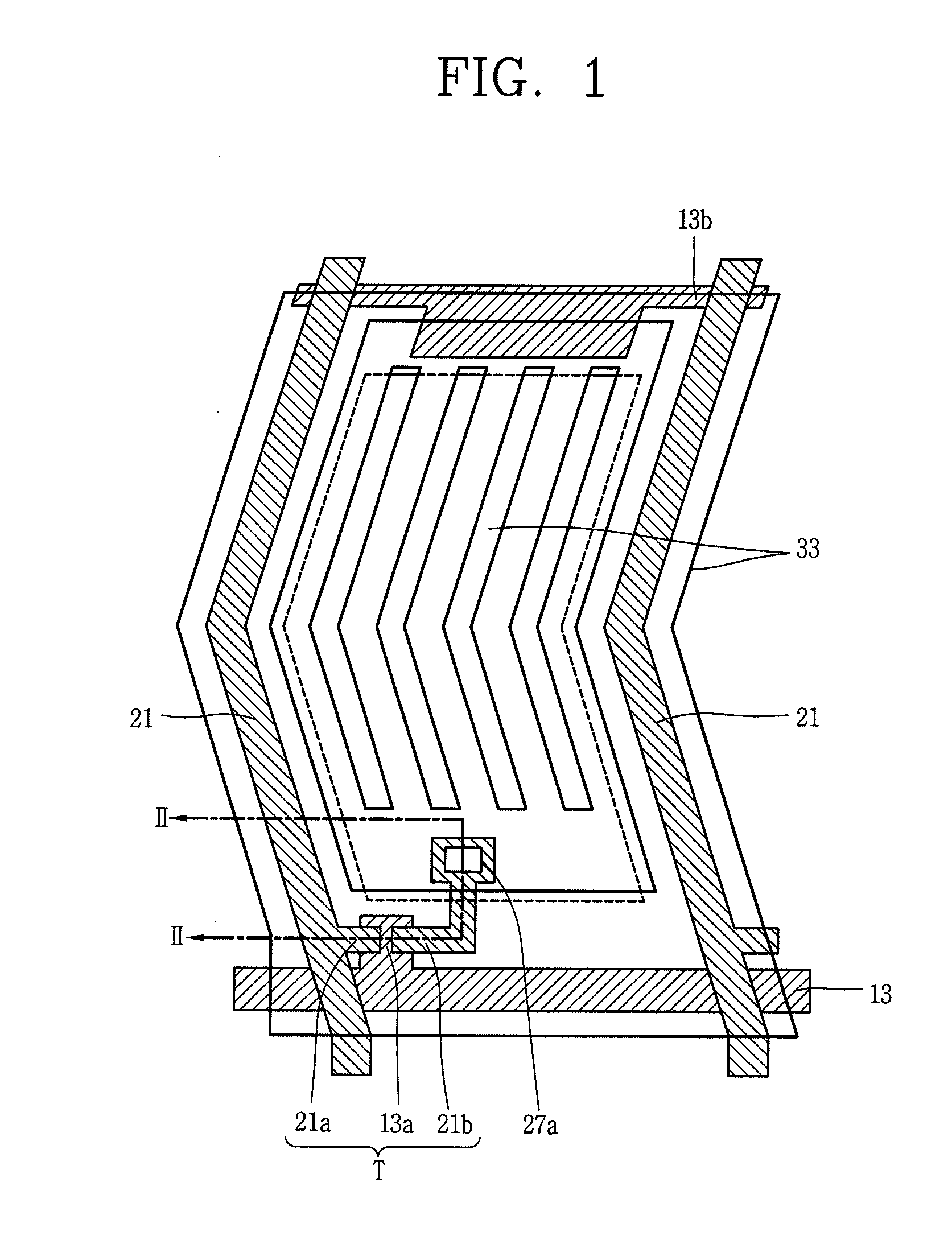
[0046]FIG. 3 is a schematic plan view illustrating a fringe field switching (FFS) mode liquid crystal display device according to the present invention.

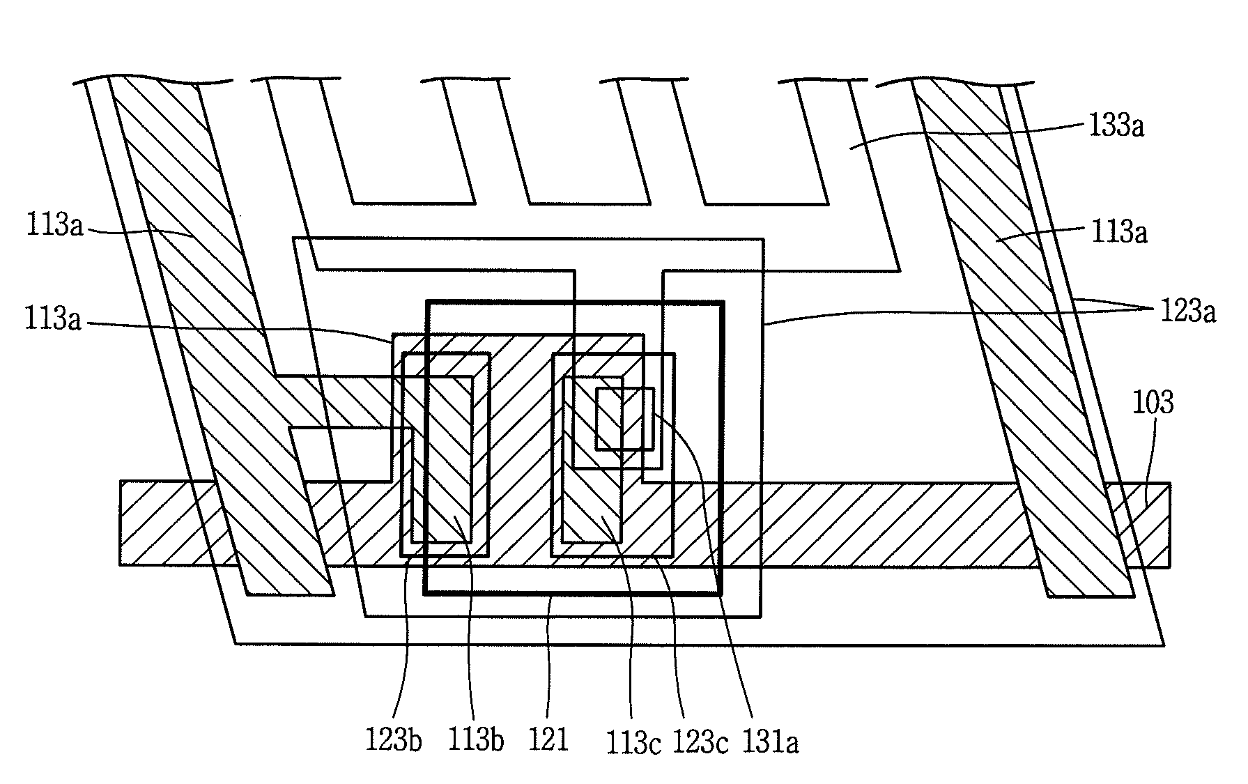
[0047]FIG. 4 is an enlarged plan view illustrating a thin-film transistor portion in a fringe field switching (FFS) mode liquid crystal display device according to the present invention.

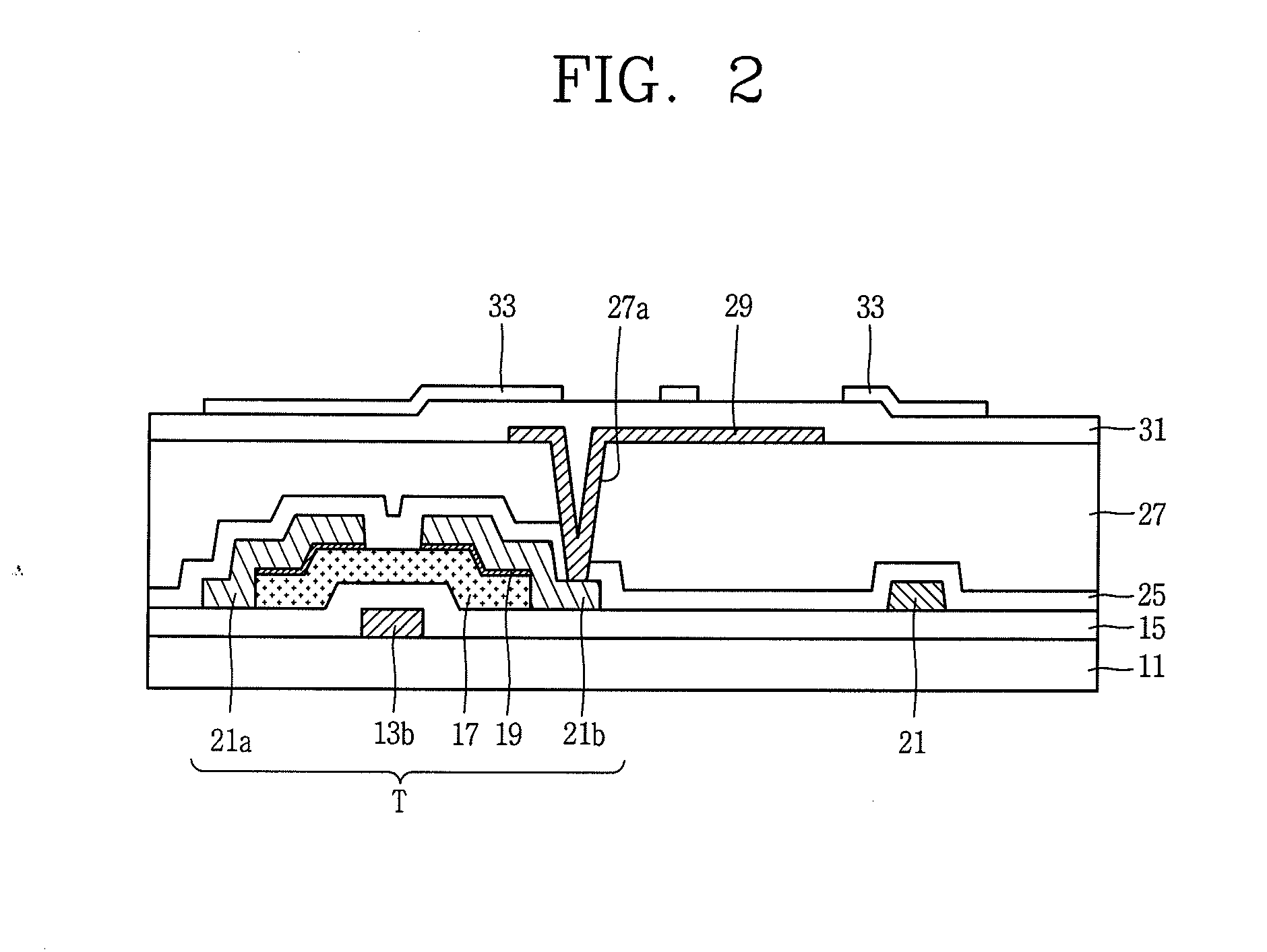
[0048]FIG. 5 is a schematic cross-sectional view illustrating a fringe field switching (FFS) mode liquid crystal display device according to the present invention, as a cross-sectional view along the line V-V of FIG. 4.

[0049]A fringe field switching (FFS) mode liquid crystal display device according to an embodiment of the present invention, as illustrated in FIGS. 3 through 5, m...


PUM


Abstract

The present invention relates to an array substrate for a fringe field switching (FFS) mode liquid crystal display device and a method for fabricating the same. The liquid crystal display device may include a gate line formed on the substrate; a data line crossed with the gate line to define a pixel region; a thin-film transistor (TFT) formed at an intersection of the gate and data line; an organic insulating layer formed to have an opening portion for exposing the TFT; a common electrode having an area formed at an upper portion of the organic insulating layer, and an auxiliary electrode pattern connected to the TFT through the opening portion; a passivation layer formed to expose the auxiliary electrode pattern connected to the TFT; and pixel electrodes electrically connected to the TFT through the exposed auxiliary electrode pattern.

Description

CROSS-REFERENCE TO RELATED APPLICATIONS[0001]This application claims the benefit of Korean Patent Application No. 10-2011-0120367, filed on Nov. 17, 2011, which is hereby incorporated by reference for all purposes as if fully set forth herein.BACKGROUND OF THE INVENTION[0002]1. Field of the Invention[0003]The present invention relates to a liquid crystal display device, and more particularly, to an array substrate for a fringe field switching (FFS) mode liquid crystal display device and a method for fabricating the same.[0004]2. Description of the Related Art[0005]In general, the driving principle of a liquid crystal display device is based on optical anisotropy and polarization of liquid crystals. Liquid crystals having an elongated structure exhibit directivity in molecular arrangement, and thus the direction of their molecular arrangement can be controlled by artificially applying an electric field to liquid crystals.[0006]Accordingly, if the molecular arrangement direction of li...

Claims


Application Information

Patent Timeline
Patent Type & Authority Applications(United States)
IPC IPC(8): H01L29/786H01L29/66
CPCH01L27/124H01L29/6675G02F1/1368H01L27/1248G02F1/134363G02F2001/134372H01L29/786G02F1/134372G02F1/1343
Inventor SHIN, DONGSUCHOI, SEUNGKYULEE, CHEOLHWAN
Owner LG DISPLAY CO LTD
Why Eureka
Try Eureka