Eureka AIR delivers breakthrough ideas for toughest innovation challenges, trusted by R&D personnel around the world.

Device for setting image acquisitoin conditions, and computer program

a technology of acquisitoin conditions and computer programs, applied in computing, instruments, electric discharge tubes, etc., can solve the problems of ineffective inspection of all the patterns on semiconductor chips, significant difficulty in finding the specified areas to be subjected to inspection using a microscope having a high resolution

Active Publication Date: 2013-05-23
HITACHI HIGH-TECH CORP
View PDF1 Cites 2 Cited by
  • Summary
  • Abstract
  • Description
  • Claims
  • Application Information

AI Technical Summary

Benefits of technology

The patent text describes a way to select the best way to capture images based on the information already captured in previous images. This means that the conditions for capturing the images can be adjusted based on changes in the process.

Problems solved by technology

In the case of inspecting processed circuit patterns in the middle of semiconductor processes, inspection of all the patterns on a semiconductor chip is ineffective.
At this time, it is significantly difficult to find the specified areas to be subjected to the inspection using a microscope having a high resolution.

Method used


Image

  • Device for setting image acquisitoin conditions, and computer program
  • Device for setting image acquisitoin conditions, and computer program
  • Device for setting image acquisitoin conditions, and computer program

Examples


embodiment 1

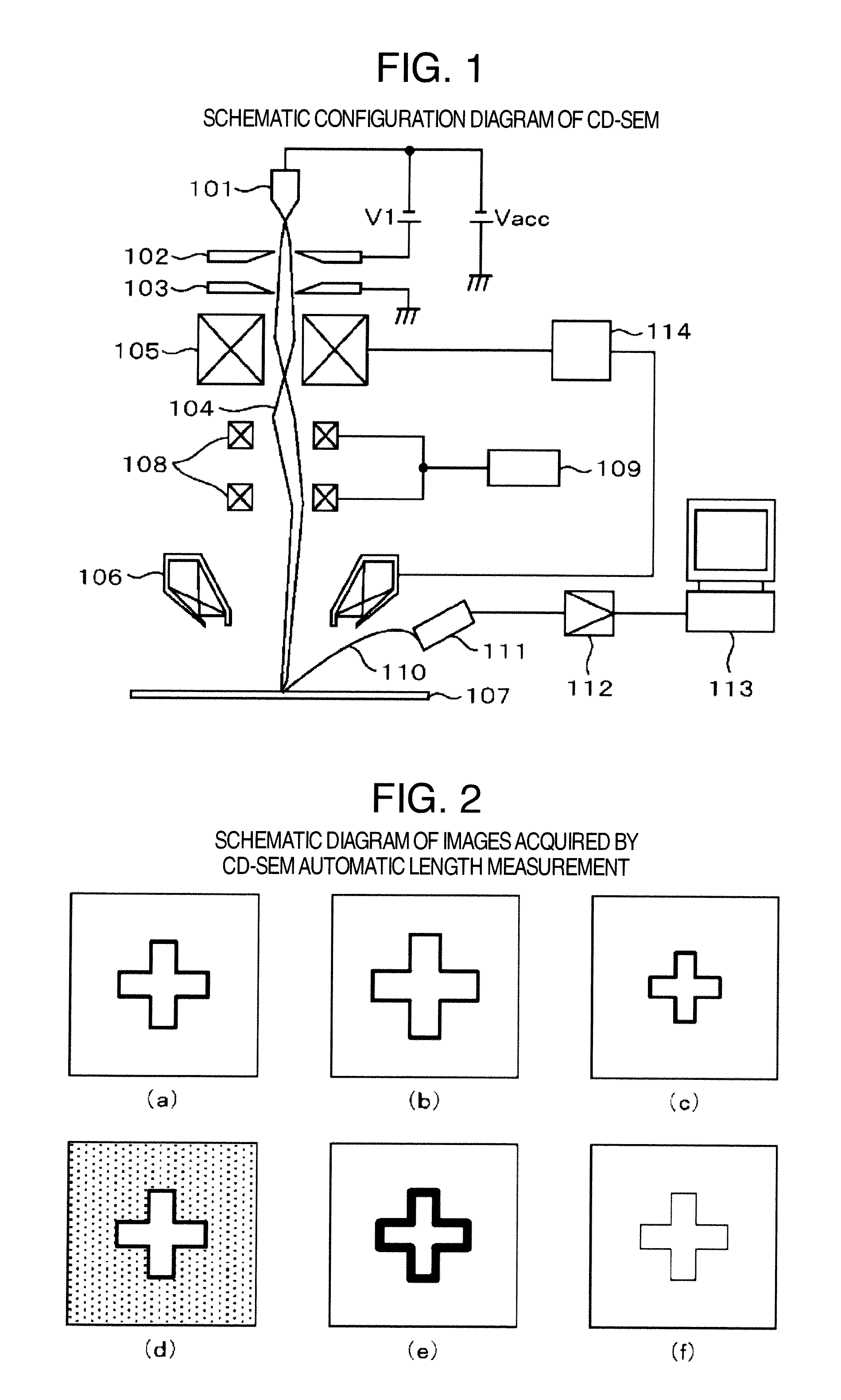
[0040]FIG. 1 is a schematic configuration diagram of a CD-SEM. A primary electron beam 104 drawn from a negative pole 101 by a voltage V1 applied to a first positive pole 102 is accelerated by a voltage Vacc applied to a second positive pole 103 and travels toward a lens system on a succeeding stage. The primary electron beam 104 is converged as a minute spot on a sample 107 by a converging lens 105 and an objective lens 106 controlled by a lens control power source 114, and two-dimensionally scans the sample 107 by means of two stages of deflection coils 108.

[0041]Scanning signals for the deflection coils 108 are controlled by a deflection controller 109 in conformity with an observation magnification. A secondary electron 110 emitted from the sample by the primary electron beam 104 scanning the sample 107 is detected by a secondary electron detector 111. Information on the secondary electron detected by the secondary electron detector 111 is amplified by an amplifier 112 and displ...

embodiment 2

[0061]On the automatic length measurement file in the CD-SEM, it is determined whether template matching succeeds or not according to the acceptance, as described above. In the case where the matching success rate is set to have priority, the acceptance may sometimes become higher than necessary. Automatic determination of the acceptance will be described in detail with reference to FIG. 15. First, an image 1001 to be registered as a template is acquired. Next, a target pattern 1002 to be a target of image recognition in the acquired image is registered. At the same time of registering the target pattern, image recognition 1003 is performed with the target pattern in the acquired image. A first candidate score S1 with the highest score and a second candidate score S2 with the second highest score are extracted. The acceptance is calculated from S1 and S2. The acceptance is the average between S1 and S2. In the case where S1 is 800 and S2 is 300, the acceptance is 550.

[0062]Here, the...


PUM


Abstract

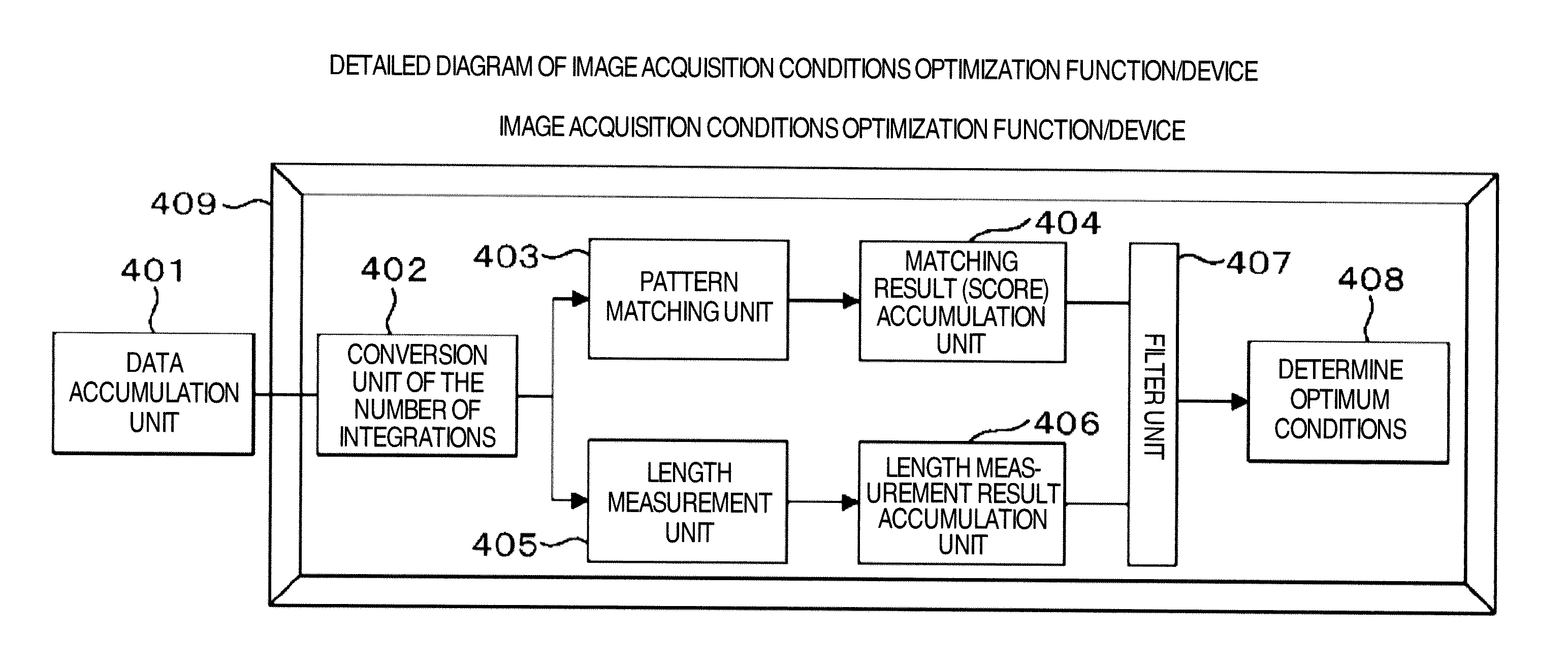
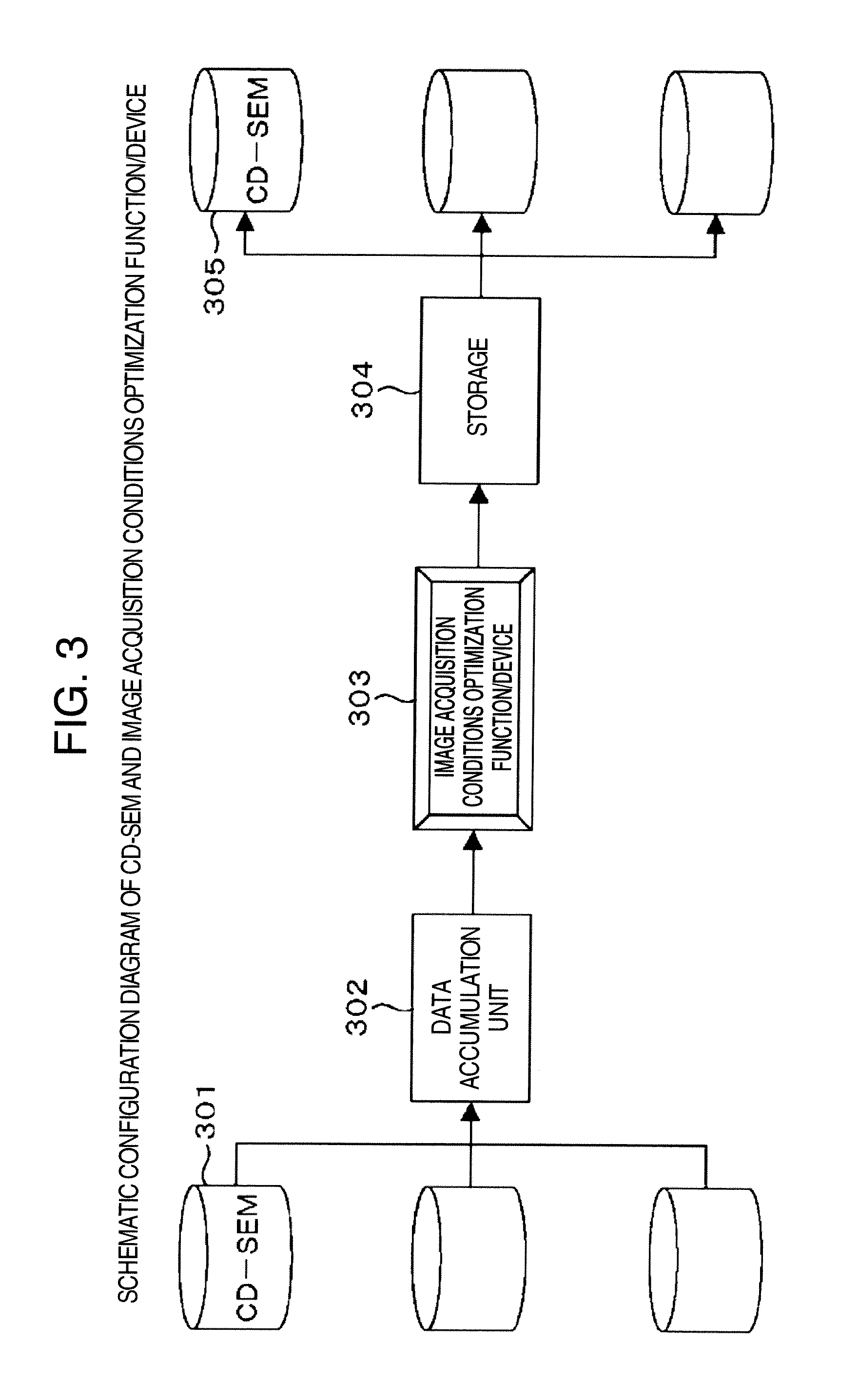
The present invention relates to a device (303) for setting image acquisition conditions for charged particle beam devices or the like. An image integration unit (402) forms a plurality of images with a number of different integrations (number of integrations 2, 4 . . . N) from one image (number of integrations N) acquired in advance. A pattern matching unit (403) matches the patterns of each of the plurality of images having a number of different integrations with template images registered in advance and then finds a score that shows the degree of matching between images. A selection unit (407) selects a number of integrations such that any variation in the scores is contained within a prescribed allowable range. The selected number of integrations is stored in a recipe of the device. Thus, it is possible to determine the number of integrations in the recipes without having to operate the device, and to set image acquisition conditions so as to allow a minimization of the processing time while maintaining a sufficient S / N ratio.

Description

TECHNICAL FIELD[0001]The present invention relates to a device for setting image acquisition conditions, such as a charged particle beam device, typified by a scanning electron microscope, and a computer program. In particular, the present invention relates to a device and a computer program that set device conditions of a device of forming an image by integrating signals.BACKGROUND ART[0002]Recently, semiconductor processes have become further finer. Fine patterns are measured and inspected using a microscope. Images of processed patterns are taken by the microscope and displayed on a display, and inspection and measurement (which hereinafter may be simply referred to as “inspection”) are performed using an image processing technique.[0003]In the case of inspecting processed circuit patterns in the middle of semiconductor processes, inspection of all the patterns on a semiconductor chip is ineffective. Accordingly, areas where a malfunction tends to occur in the process or occurred...

Claims


Application Information

Patent Timeline
Patent Type & Authority Applications(United States)
IPC IPC(8): G06K9/20
CPCG06K9/6202G06K9/20H01J37/28H01J37/222G06V10/751
Inventor YAMADA, YAKARIKONDO, AKEMI
Owner HITACHI HIGH-TECH CORP
Why Eureka
Eureka Blog
Learn More