Method for reducing image artifacts produced by a CMOS camera

a technology of image artifacts and camera, applied in the field of system and method for reducing image artifacts, can solve the problems of low-cost imagers, insufficient quality of embedded image correction software, and inability to provide solutions that are often impractical, and achieve superior image artifact reduction, reduce several image artifacts, and reduce image artifacts

Inactive Publication Date: 2013-05-23
GE HEALTHCARE BIO SCI CORP
View PDF4 Cites 6 Cited by
  • Summary
  • Abstract
  • Description
  • Claims
  • Application Information

AI Technical Summary

Benefits of technology

[0008]The present invention provides image processing algorithms and systems for reducing several image artifacts produced by a CMOS camera in a monochromatic image. The present invention further provides algorithms and systems for reducing such image artifacts in a line confocal fluorescent imager which uses a CMOS camera as the optical detector. The methods and systems offer superior image artifact reduction in comparison with the built-in functions by the manufacturer of CMOS camera. More specifically, the system and method subtract dark current and reduce CMOS artifacts for all images. Artifacts reductions include RGB channel offset mismatch and random row offset. Optionally, artifacts reductions also include random column offset and gain, as well as correction of defective pixels.

Problems solved by technology

However, the embedded image correction software does not provide sufficient quality images.
These solutions are often impractical, particularly for low-cost imagers.

Method used


Image

  • Method for reducing image artifacts produced by a CMOS camera
  • Method for reducing image artifacts produced by a CMOS camera
  • Method for reducing image artifacts produced by a CMOS camera

Examples


Embodiment Construction

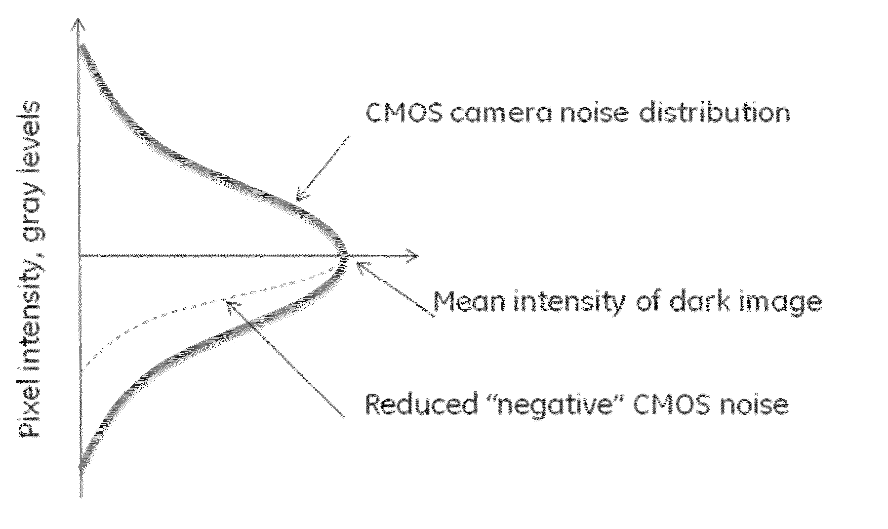
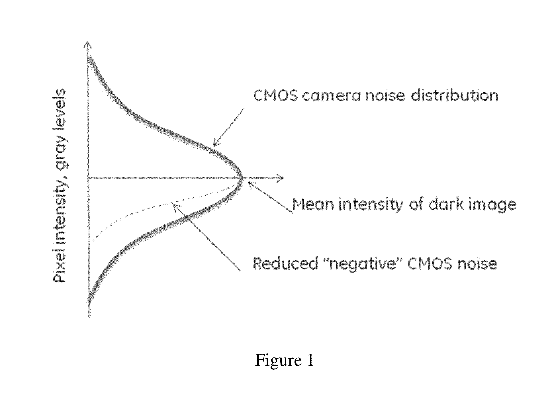
[0019]A new laser line confocal imager is developed based on a technology of pixel-based confocality implemented using a rolling shutter feature of conventional CMOS cameras. The CMOS camera produces several specific image artifacts that need to be corrected / reduced in raw images to improve visual image quality of obtained images. These include RGB channel offset mismatch and random row offset. Preferably, the random column offset and gain should also be reduced. Moreover, correction of defective pixels should be provided as an option.

[0020]The embodiments may be implemented within an image processor associated with a pixel array in an image capture device or may be implemented in a separate image processor which receives captured image data.

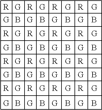
[0021]The CMOS array detectors are active column detectors. As an example, the principle of operation for the mt9m001 CMOS array imager (½″, 1.3 Megapixel, Micron Technologies) is described here:[0022]To read a row, the row is addressed.[0023]Fo...


PUM


Abstract

The present invention relates to a system and method for reducing image artifacts for a CMOS camera used as an optical detector for a line confocal fluorescent imager. The method for reducing image artifacts in a monochromatic image comprises subtracting RGB channel offset mismatch; and correcting random row offset for each row. Preferably, the method also comprises correcting random column offset and gain. Optionally, the method also comprises clipping of defective pixels, and/or subtracting dark current. When the monochromatic image is a fluorescence image, the method also comprises a step of compressing CMOS camera noise. Also provided are a system for reducing image artifacts in a monochromatic image from a CMOS camera, as well as an image artifact reduction system for a CMOS camera-based line confocal fluorescent microscope.

Description

CROSS-REFERENCE TO RELATED APPLICATIONS[0001]This application claims priority to U.S. provisional patent application Ser. No. 61 / 369,093 filed July 30, 2010; the disclosure of which is incorporated herein by reference in its entirety.FIELD OF THE INVENTION[0002]The present invention relates to a system and method for reducing image artifacts. Specifically, the invention relates to a system and method for reducing image artifacts when a CMOS camera is used as an optical detector for a line confocal fluorescent imager.BACKGROUND OF THE INVENTION[0003]CMOS imagers (complementary metal-oxide-semiconductor imagers) are well known. Images generated from CMOS or other imagers typically comprise thousands or even millions of picture elements called “pixels” arranged in rows and columns (array). Pixel cells contain photosensors. Each pixel cell produces a signal corresponding to the intensity of light impinging on its photosensor when an image is focused on the array by one or more lenses. T...

Claims


Application Information

Patent Timeline
Patent Type & Authority Applications(United States)
IPC IPC(8): G06T5/00
CPCH04N1/409G06T5/005G06T5/00H04N5/357H04N25/60
Inventor FOMITCHOV, PAVEL A.BULA, WITOLDZARATE, CARLOSZHANG, YANG
Owner GE HEALTHCARE BIO SCI CORP
Why Eureka
Try Eureka