Organic semiconductor composition, organic thin film, and organic thin film transistor having same
a technology of organic semiconductor materials and semiconductor compositions, applied in thermoelectric devices, triarylamine dyes, chemistry apparatus and processes, etc., can solve the problems of field-effect mobility (mobility, organic semiconductor materials have not reached the mobility level), and achieve high carrier transport properties, uniform characteristics, and high carrier transport properties
- Summary
- Abstract
- Description
- Claims
- Application Information
AI Technical Summary
Benefits of technology
Problems solved by technology
Method used
Image
Examples
example 1
[0134]First, each of the compound represented by Formula (8) (a high molecular weight compound (8)) as a high molecular weight compound having carrier transport property, and a compound represented by above-mentioned Formula (1d) (a low molecular weight compound (1d)) as a low molecular weight compound was prepared.
[0135]The high molecular weight compound (8) was synthesized by mixing such monomers as 9,9-dioctylfluorene-2,7-bis(dimethyl borate) and N,N-bis(4-bromophenyl)-N-(4-sec-butyphenyl) at a ratio of 50:50 and by a method described in Japanese Patent No. 4375820. The high molecular weight compound (8) had weight average molecular weight of 351,000 in terms of polystyrene, and number average molecular weight of 85,000. Incidentally, n in Formula (8) represents the repeating number of the structure in parentheses, which is the number corresponding to the case where the weight average molecular weight and the number average molecular weight of the compound give above-mentioned va...
example 2
[0143]An organic thin film transistor was produced in the same manner as in Example 1, except for employing the low molecular weight compound (1b) in place of the low molecular weight compound (1d). For five organic thin film transistors, transistor characteristics were measured under such conditions that the source-drain voltage Vsd was set to be −40 V and the gate voltage Vg was varied from 20 to −40 V. The median value of field-effect mobility (mobility) calculated from such measurement results was 0.13 cm2 / Vs, and the coefficient of variation was 38.6%.
example 3
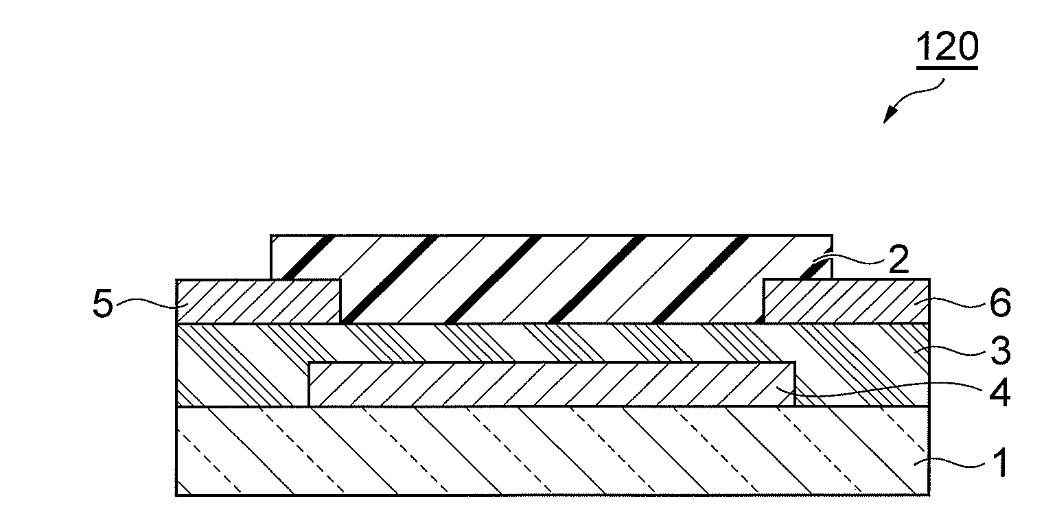
[0144]An organic thin film transistor was produced in the same manner as in Example 1, except for employing a compound represented by Formula (9) (a high molecular weight compound (9)) as the high molecular weight compound having a carrier transport property. Incidentally, the high molecular weight compound (9) is a compound that gives a field-effect mobility of 0.0035 cm2 / Vs, when an organic thin film transistor with a structure shown in FIG. 13 including an organic thin film (an organic semiconductor layer) composed of only the compound.
[0145]In the synthesis of the high molecular weight compound (9), first, 9,9-dioctylfluorene-2,7-bis(dimethyl borate) and 5,5′-dibromo-2,2′-bithiophene being monomers were mixed at a ratio of 50:50, which was used for implementing a method described in Japanese Patent Laid-Open No. 2009-108228 to give the high molecular weight compound (9). The high molecular weight compound (9) had weight average molecular weight of 61,000 in terms of polystyrene,...
PUM
| Property | Measurement | Unit |
|---|---|---|
| thickness | aaaaa | aaaaa |
| contact angle | aaaaa | aaaaa |
| thickness | aaaaa | aaaaa |
Abstract
Description
Claims
Application Information
 - R&D
- Intellectual Property
- Life Sciences
- Materials
- Tech Scout
- Unparalleled Data Quality
- Higher Quality Content
- 60% Fewer Hallucinations
Browse by: Latest US Patents, China's latest patents, Technical Efficacy Thesaurus, Application Domain, Technology Topic, Popular Technical Reports.
© 2025 PatSnap. All rights reserved.Legal|Privacy policy|Modern Slavery Act Transparency Statement|Sitemap|About US| Contact US: help@patsnap.com


