High Electron Mobility Transistors with Multiple Channels

a technology of electron mobility and transistor, applied in the field of gallium nitride (gan) based high electron mobility transistor, can solve the problems of controllability issue or lattice damage problem, degrade rf amplification capability, deplete the 2deg underneath the gate region, etc., and achieve the effect of enhancing current carrying capability and high electron mobility transistor

Active Publication Date: 2013-06-06
MITSUBISHI ELECTRIC CORP +1
View PDF2 Cites 34 Cited by
  • Summary
  • Abstract
  • Description
  • Claims
  • Application Information

AI Technical Summary

Benefits of technology

[0011]An objective of present invention is to provide a high electron mobility transistor (HEMT) having enhanced current carrying capability. It is a further object of some embodiments to

Problems solved by technology

Those techniques can deplete the 2DEG underneath the gate region but suffer from either controllability issue or lattice damage problem.
However, despite the increased performance of the N-polar devices, the drive current und

Method used


Image

  • High Electron Mobility Transistors with Multiple Channels
  • High Electron Mobility Transistors with Multiple Channels
  • High Electron Mobility Transistors with Multiple Channels

Examples


Embodiment Construction

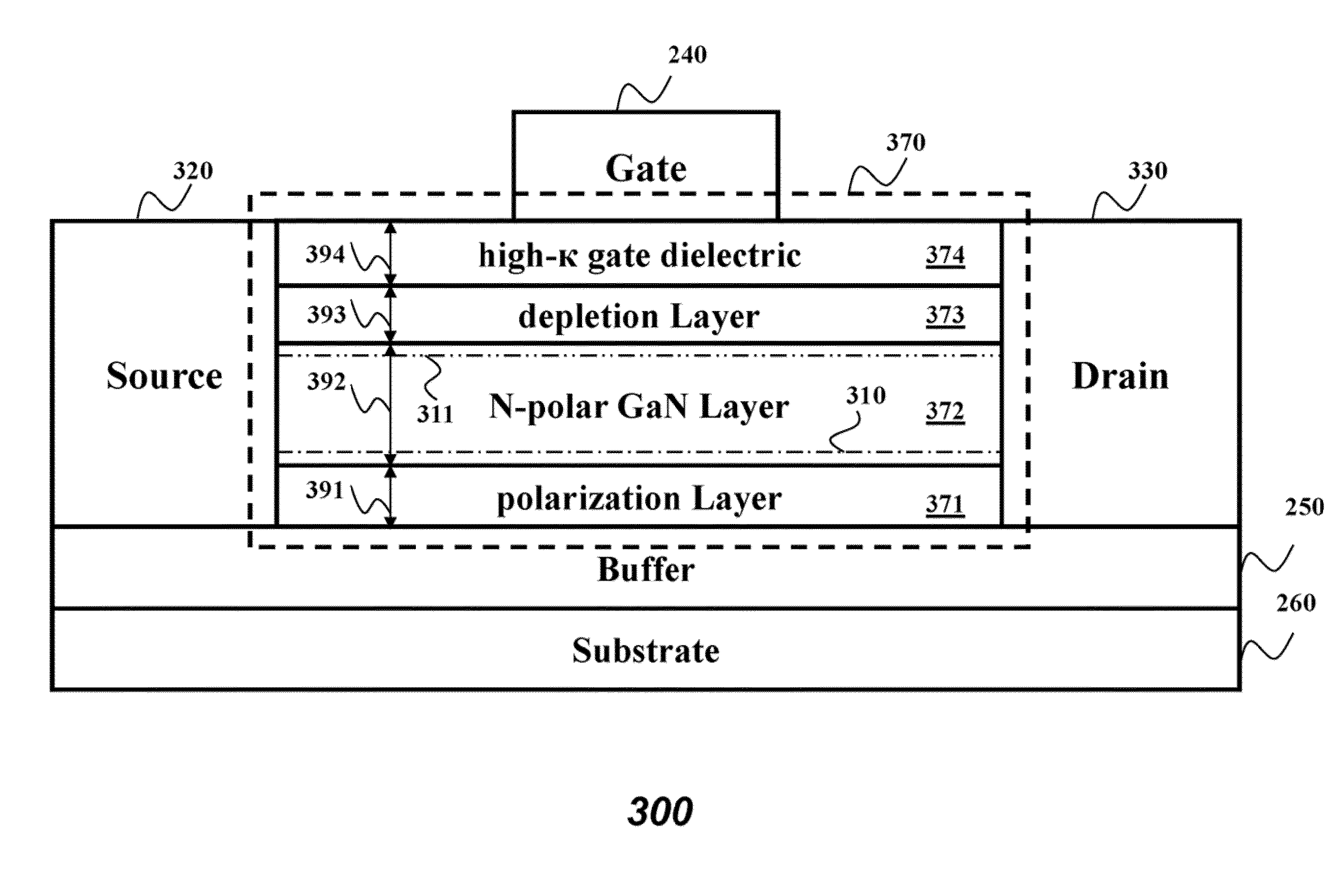
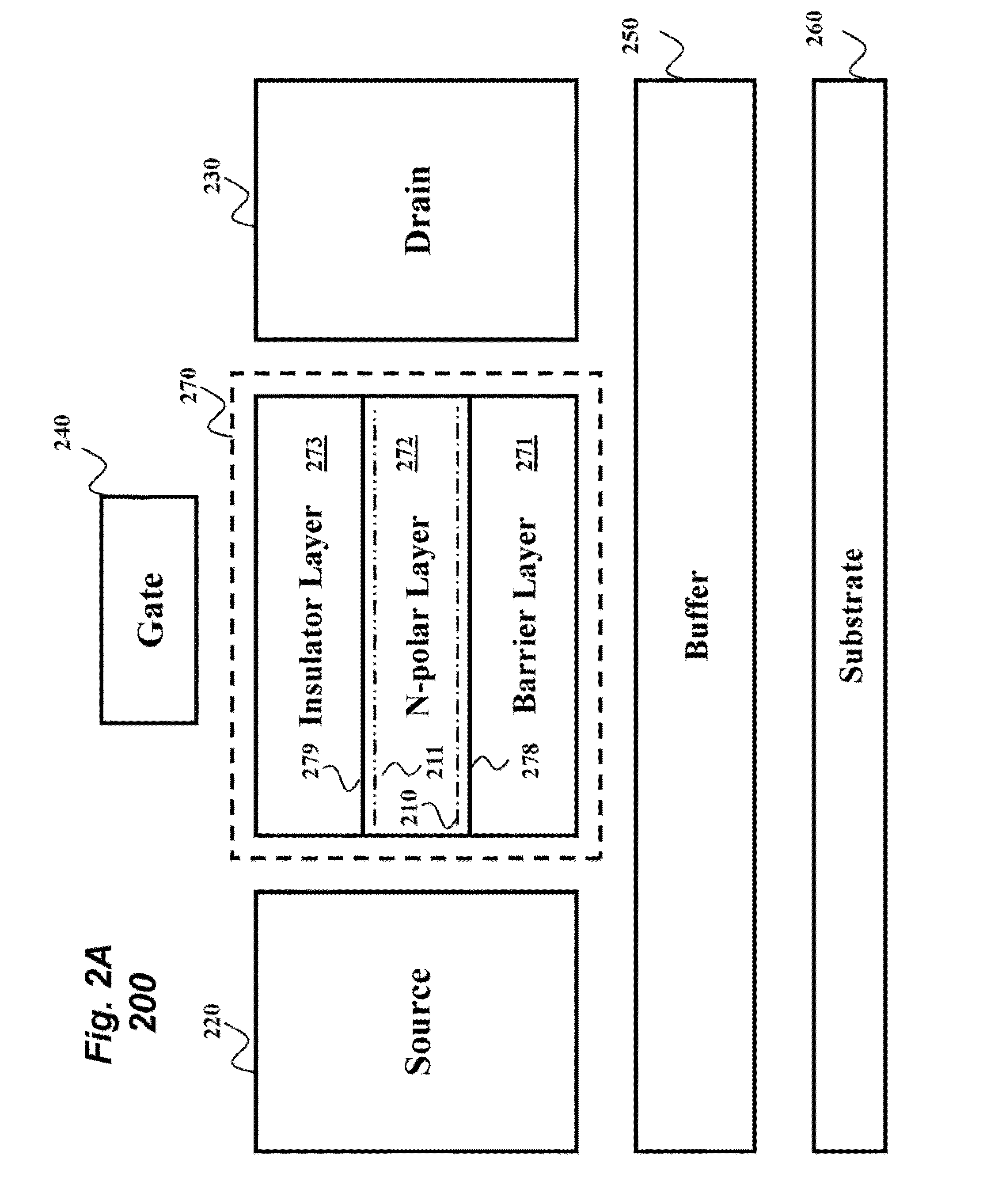
[0029]FIG. 2A shows a schematic of a device 200 designed according to embodiments of the invention. The device 200 can be a high electron mobility transistor (HEMT) device. The device includes a source 220 for transmitting an electronic charge through a conduction path, a drain 230 for receiving the electronic charge, a stack 270 for providing at least part of the conduction path, a gate 240 operatively connected to the stack for controlling a conduction of the electronic charge. The device can also include a buffer 250 and a substrate 260. The stack 270 can be an N-polar stack 270 that includes a barrier layer 271, an N-polar layer 272, and an insulator layer 273 selected such that, during the operation of the device 200, an inversion carrier channel 210 and a two-dimensional electron gas (2DEG) channel 211 are formed in one N-polar layer 272. The channels 210 and 211 formed at least part of the conductive path between the source and the drain.

[0030]Some embodiments of the inventio...


PUM


Abstract

A device includes a source for transmitting an electronic charge through a conduction path; a drain for receiving the electronic charge; a stack for providing at least part of the conduction path; and a gate operatively connected to the stack for controlling a conduction of the electronic charge. The stack includes an insulator layer, an N-polar layer and a barrier layer selected such that, during an operation of the device, the conduction path formed in the N-polar layer includes a two-dimensional electron gas (2DEG) channel and an inversion carrier channel.

Description

RELATED APPLICATION [0001]This application claims priority from a provisional application 61 / 566,791 entitled, “High Electron Mobility Transistors with Multiple N-Polar GaN Channels,” filed Koon Hoo Teo et al. on Dec. 5, 2011.FIELD OF THE INVENTION [0002]The present invention relates generally to gallium nitride (GaN) based high electron mobility transistors (HEMTs), and more particularly to transistors with multiple conductive channels.BACKGROUND OF THE INVENTION[0003]High electron mobility transistor (HEMT), also known as heterostructure FET (HFET) or modulation-doped FET (MODFET), is a transistor incorporating a junction between two materials with different band gaps, i.e., a heterojunction, as the channel. The heterojunction can be contrasted with a doped layer that generally used by MOSFET. As used herein, the heterojunction is the interface that occurs between two layers or regions of dissimilar crystalline semiconductors or other materials. A commonly used material combinatio...

Claims


Application Information

Patent Timeline
IPC IPC(8): H01L29/778G05F1/00
CPCH01L29/7783H01L29/2003H01L2924/0002H01L2924/00
Inventor TEO, KOON HOOFENG, PEIJIEDUAN, CHUNJIEOISHI, TOSHIYUKIMASATOSHI, NAKAYAMA
Owner MITSUBISHI ELECTRIC CORP
Why Eureka
Try Eureka