Spin-wave waveguide and spin wave operation circuit

a technology of operation circuit and spin wave, which is applied in waveguides, magnetic bodies, instruments, etc., can solve the problems of inability to make use of asynchronous information processing methods, large applicability restrictions, and complex elements, and achieve the effect of ultra-low power consumption

Inactive Publication Date: 2013-06-13
HITACHI LTD
View PDF2 Cites 9 Cited by
  • Summary
  • Abstract
  • Description
  • Claims
  • Application Information

AI Technical Summary

Benefits of technology

[0023]Thus, the use of the present invention can provide a spin-wave waveguide ultra-low power consumption, compatible with an existing synchronous operation circuit, and an operation circuit using the spin-wave waveguide.

Problems solved by technology

However, the spin-wave operation circuit described as above has the following problem.
2141-2150 (2008)} is not provided with a mechanism whereby an operation is sequentially progressed according to a clock, so that it is impossible to make use of asynchronous information-processing method that is in the mainstream at present, and applicability is considerably restricted.
However, with the operation circuit described as above, the ME effect element used for writing, and excitation of the spin wave is an element made up by coupling a ferromagnetic material to a ferroelectric material, so that the ME effect element goes into complex actions such as (1) distortion being induced in the ferroelectric material by applying a voltage to the ferroelectric material, and (2) magnetic anisotropy of the ferromagnetic material being modulated due to a magnetostriction effect caused by the distortion as induced.
A high-performance ME effect element operating at room temperature has not been available up to now.

Method used


Image

  • Spin-wave waveguide and spin wave operation circuit
  • Spin-wave waveguide and spin wave operation circuit
  • Spin-wave waveguide and spin wave operation circuit

Examples


first embodiment

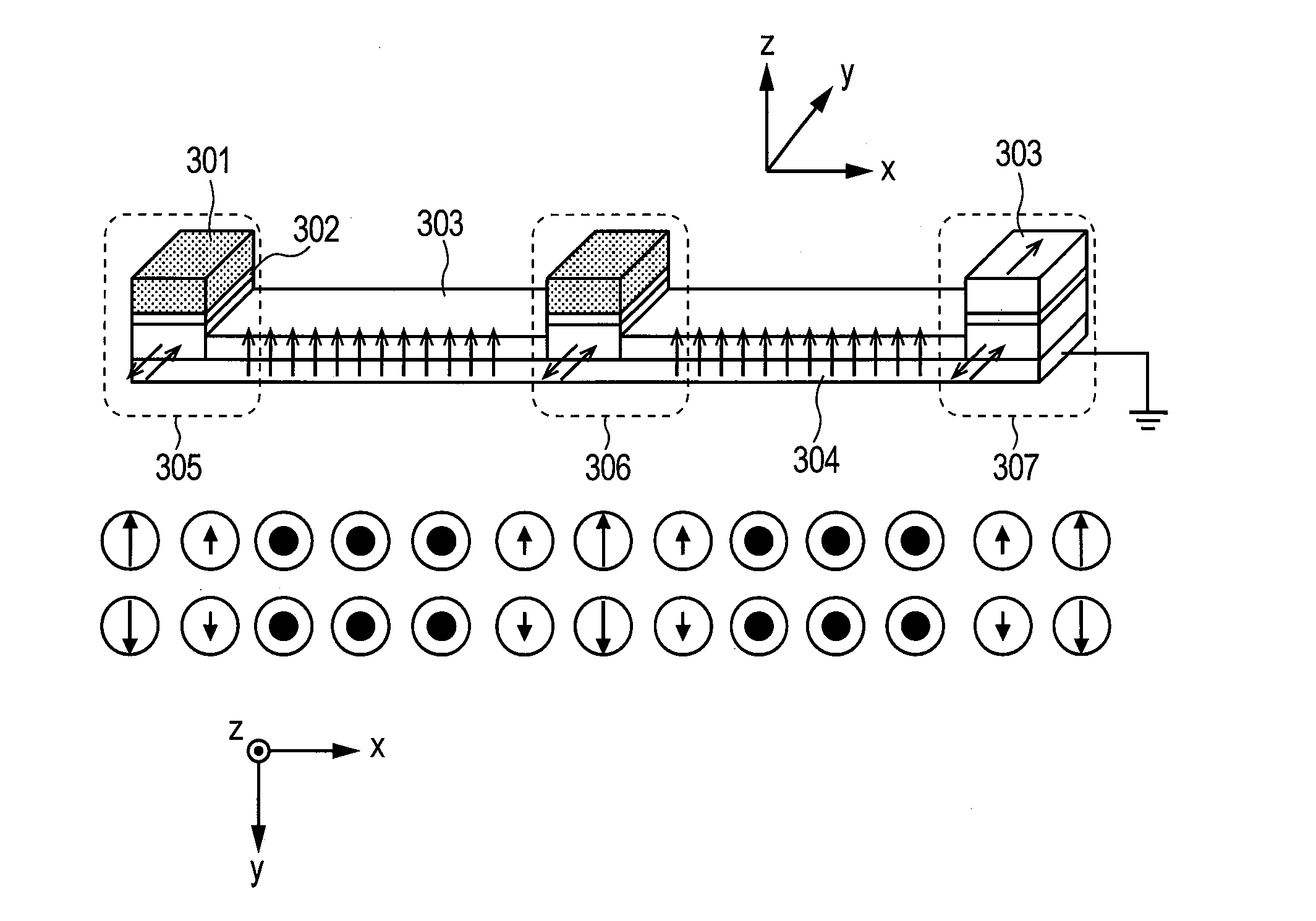
[0036]FIG. 3 is a view showing a first embodiment of a spin-wave waveguide according to the invention.

[0037]Reference numeral 301 denotes an electrode, 302 an insulating film, 303 a ferromagnetic filmmaking up a spin-wave waveguide, and 304 a substrate film. Reference numeral 305 denotes an information input part, 306 a primary information-recording part, and 307 an information regeneration part. The ferromagnetic film 303 is substituted for the electrode 301 at 307, and 307 serves as a so-called ferromagnetic tunneling junction (MTJ).

[0038]Further, description is given hereinafter with reference to an xyz coordinate system shown in FIG. 3. With the present invention, a direction vertical to the film surface indicates the z-axis direction, and a direction parallel with the film surface indicates the direction within the x-y plane. This definition is exactly identical to that given with reference to FIGS. 1, 2, respectively.

[0039]Directions of magnetization in respective regions are ...

second embodiment

[0071]FIG. 10 is a schematic diagram showing a second embodiment of a spin-wave waveguide according to the invention. Reference numeral 1001 denotes an electrode, 1002 an insulating film, 1003 a ferromagnetic film having magnetic anisotropy within a film surface, 1004 a ferromagnetic film making up a spin-wave waveguide, and 1005 a substrate film. Reference numeral 1006 denotes an information input part, 1007 a primary information-recording part, and 1008 an information regeneration part. At 1008, the ferromagnetic film 1003 is substituted for the electrode 1001, and the primary information-recording part 1007 serves as the so-called ferromagnetic tunneling junction (MTJ).

[0072]In FIG. 10, a region 1006 is linked with the waveguide part 1004 where a direction of the easy axis of magnetization is perpendicular to the film surface via the same constituent material although the easy axis of magnetization of the ferromagnetic film 1003 is oriented in the longitudinal direction, so that ...


PUM


Abstract

A spin-wave waveguide includes a ferromagnetic thin film resembling a wire in shape. A part of the ferromagnetic thin film, large in film thickness, is formed at one end of the ferromagnetic thin film, and a part of the ferromagnetic thin film, small in film thickness, and a part of the ferromagnetic thin film, large in film thickness, are alternately formed on the same plane, for at least not less than one cycle. A part of the ferromagnetic thin film, large in film thickness, is formed at the other end of the ferromagnetic thin film, wherein an insulating film, and an electrode film are stacked in this order on the ferromagnetic thin film in the part of the ferromagnetic thin film, large in film thickness.

Description

CLAIM OF PRIORITY[0001]The present application claims priority from Japanese patent application JP 2011-269558 filed on Dec. 9, 2011, the content of which is hereby incorporated by reference into this application.FIELD OF THE INVENTION[0002]The present invention relates to a waveguide, and an element, using a spin wave as an information-transmission medium, and an operation circuit using the waveguide.BACKGROUND OF THE INVENTION[0003]While information content to be processed in a unit time has exponentially increased along with an explosive development in the information society, a dramatic decrease in energy made available for use in information-processing has been in strong demand from the standpoint of the global environment, and energy constraints. With a semiconductor operation element based on a CMOS, available up to now, performance has increased along with miniaturization, however, an increase in power consumption, induced by an increase in leakage current loss increasing du...

Claims


Application Information

Patent Timeline
Patent Type & Authority Applications(United States)
IPC IPC(8): H01P3/16
CPCH01P3/165H01F10/3254H01F10/3286G11C11/16H01L43/08G11C11/161G11C11/1675H10B61/00H10N59/00H10N50/10
Inventor ITO, KENCHIYAMADA, MASAKIOGAWA, SUSUMU
Owner HITACHI LTD
Why Eureka
Try Eureka