
Radiation detection apparatus
a technology of radiographic equipment and phosphor materials, applied in the direction of instruments, radiation measurement, measurement devices, etc., can solve the problems of difficult to obtain high-resolution radiographic images, difficult to uniformly mix different phosphor materials, etc., and achieve the effect of stable manufacturing
- Summary
- Abstract
- Description
- Claims
- Application Information
AI Technical Summary
Benefits of technology
Problems solved by technology
Method used
Image

Examples
first embodiment
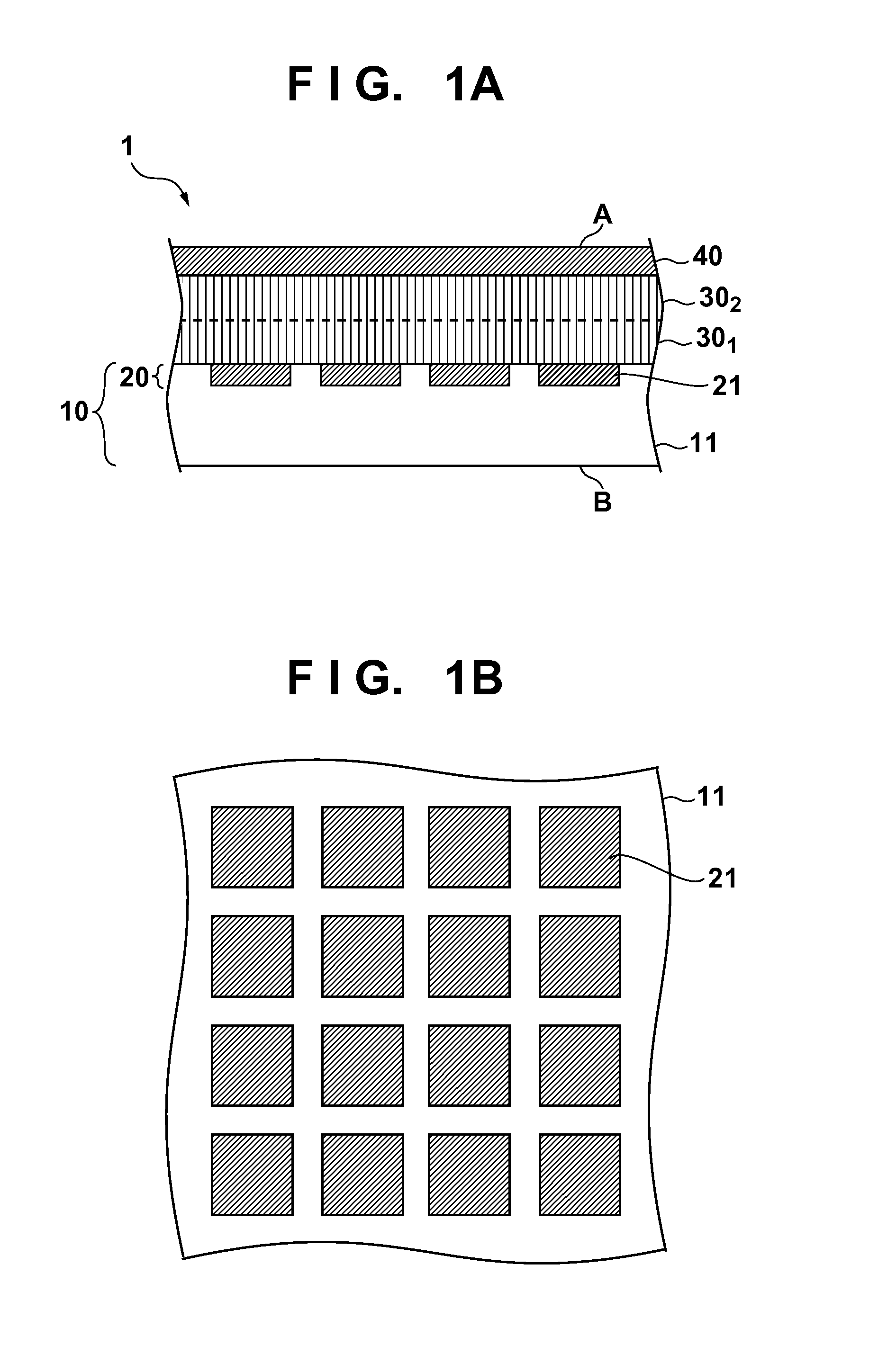
[0020]A radiation detection apparatus 1 according to the first embodiment will be described with reference to FIGS. 1A to 6. FIGS. 1A and 1B are views for explaining the radiation detection apparatus 1. FIG. 1A is a schematic view of the sectional structure of the radiation detection apparatus 1. FIG. 1B is a schematic view of the planar layout of the radiation detection apparatus 1.
[0021]The radiation detection apparatus 1 can include a sensor panel 10, a first scintillator layer 301, and a second scintillator layer 302. The sensor panel 10 can include a sensor unit 20 having a plurality of photoelectric converters 21 two-dimensionally arranged on a substrate 11. The first scintillator layer 301 is disposed on the sensor panel 10. The second scintillator layer 302 is disposed on the first scintillator layer 301. The first and second scintillator layers 301 and 302 convert radiations (including electromagnetic waves such as X-rays, α-rays, β-rays, and γ-rays) into light beams. In ge...
second embodiment
[0031]A radiation detection apparatus 2 according to the second embodiment will be described with reference to FIGS. 7A to 10. As exemplified by FIG. 7A, a sensor panel 10′ of the radiation detection apparatus 2 can include an insulating substrate 60 made of glass or the like, a TFT switch 70, an interlayer dielectric layer 80, a contact hole 90, and a sensor unit 20′. Amorphous silicon is used for the sensor unit 20′, on which a plurality of photoelectric converters 100 are two-dimensionally arranged. The TFT switch 70 can be disposed on the insulating substrate 60. The interlayer dielectric layer 80 is disposed to cover the insulating substrate 60 and the TFT switch 70. The contact hole 90 can be formed in the interlayer dielectric layer 80 in a region on the TFT switch 70. The photoelectric converter 100 can be connected to the contact hole 90. A passivation layer 110 can be provided so as to cover the interlayer dielectric layer 80 and the photoelectric converter 100. In additio...
PUM
 Abstract
Description
Claims
Application Information