Semiconductor package with improved thermal properties

Active Publication Date: 2013-07-18
NXP BV
17 Cites 3 Cited by

AI-Extracted Technical Summary

Problems solved by technology

Ever more input and output signals on ever smaller silicon chip areas has in part lead to the strain in the BE process to keep up with miniaturization.
Moreover, there are additional constraints on the BE process caused by a need for smaller footprints and smaller form factors (physical dimensions) of the semiconductor packages.
Although this is very much dependant on the type of application, it can be seen that high frequency applications with increasing miniaturization at some point will test the boundaries, resulting in an increased jun...

Method used

[0041]FIG. 2 shows a cross sectional view of one example of a semiconductor package 10 of the kind described in FIG. 1. In this embodiment, the back side of the silicon substrate 6 coincides with the lower side of the semiconductor package 10. This facilitates fabrication of a heat spreader 14 at the lower side of the semiconductor package 10 where a direct thermal contact between the backside of the semiconductor substrate 10 to the heat spreader 14 is aided. The active side of the semiconductor substrate 6, as well as the redistribution layer 8 on top of the semiconductor package 10, may be protected from the environment by a passivation or overmolding layer 18. This layer can provide additional protection to the device against, for example, moisture.
[0042]FIG. 3 shows a cross sectional view of another example of a semiconductor package 10 of the kind described in FIG. 1. In this embodiment, the back side of the silicon substrate 6 is recessed with respect to the lower side of the semiconductor package 10. The recessed volume is filled with a thermally conductive material 20 up to the level of the lower side of the semiconductor package 10. The so created planar lower side of the semiconductor package 10 facilitates the fabrication of a heat spreader 14 in this embodiment. The thermally conductive material aids a good thermal coupling between the back side of the silicon substrate 6 and the heat spreader 14.
[0043]FIG. 3 shows a cross sectional view of a further example of a semiconductor package 10 of the kind described in FIG. 1. In this embodim...

Benefits of technology

[0021]The heat spreader can comprise a thermally conductive material (e.g. it can be metallic). The heat spreader can aid an enhanced thermal conductive coupling to the surface.
[0022]According to another embodiment the backside of the substrate can coincide with the surface of the lower side of the encapsulant. This can facilitate fabrication of the heat spread...

Abstract

A semiconductor package, comprises an encapsulant which contains a semiconductor substrate, the package lower side being mountable on a surface. The semiconductor substrate backside is in close proximity of the semiconductor package lower side for improved thermal conductivity to the surface. The active side of the semiconductor substrate, facing the upper side of the semiconductor package, has a plurality of die contacts. A plurality of electrically conductive interconnects are connected to the die contacts and extend to the lower side of the semiconductor package for connecting the die contacts to the surface.

Application Domain

Technology Topic

Image

  • Semiconductor package with improved thermal properties
  • Semiconductor package with improved thermal properties
  • Semiconductor package with improved thermal properties

Examples

  • Experimental program(1)

Example

[0038]Embodiments of the present invention are described in the following with reference to the accompanying drawings.
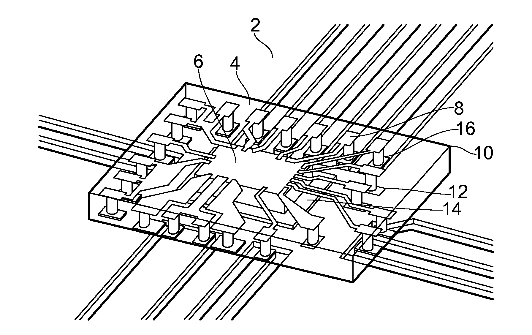
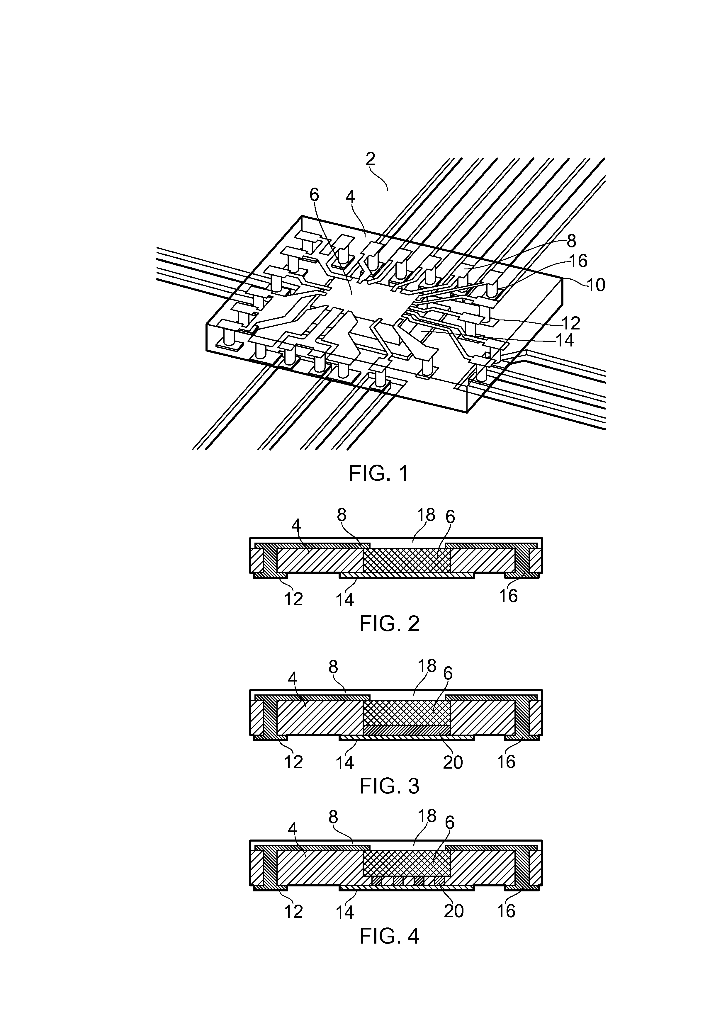
[0039]FIG. 1 shows an example of a semiconductor package 10 according to an embodiment of the invention. As shown in FIG. 1, the semiconductor package 10 includes a semiconductor substrate 6, with in this example the active side facing upward. As is well known in the art, active side of a semiconductor substrate is typically the side of the substrate that includes components such as transistors, capacitors and other circuitry. The semiconductor substrate 6 is embedded in an encapsulant 4, which is electrically insulating and which can provide mechanical support and protection for the semiconductor substrate 6. Electrically conductive interconnects are connected to the semiconductor substrate 6 at the upper side of the semiconductor package 10. These interconnects are laterally spread out and fed through the encapsulant 4 to a pad ring 12 located at a lower side of the encapsulant 4. In particular, in the present embodiment, a redistribution layer 8 connects to the die contacts (not shown in FIG. 1), which are part of the semiconductor substrate 6. The redistribution layer 8 extends the electrical conductive interconnects from the die contacts on the substrate, towards the outer perimeter of the semiconductor package 10. It will be understood that the positioning of the outer part of the redistribution layer 8 is not limited to an evenly spaced configuration along the perimeter of the semiconductor package 10. An uneven spacing along the perimeter or an extension of the electrically conductive interconnects from the die contacts to a position anywhere on the surface of the semiconductor package 10 is also contemplated.
[0040]The electrically conductive interconnects also pass through the encapsulant via vertically oriented conductive portions 16. The vertically oriented conductive portions 16 connect the redistribution layer 8 at the upper side of the semiconductor package 10 to the pad ring 12 located at the lower side of the semiconductor package 10. A heat spreader 14 is located near the lower side of the semiconductor package 10, and is thermally connected to the back side of the silicon substrate 6. The described embodiment of the semiconductor package 10 allows for a physical separation of the electrically conductive interconnects and the thermal coupling to a surface where the semiconductor package 10 can be mounted on, for example a printed circuit board 2. The insulating encapsulant 4 ensures the integrity of separate isolated electrically conductive interconnects, as well as an electrically isolated heat spreader 14. Similarly as the pad ring 12 can be connected to a printed circuit board 2, so can the heat spreader 14. The printed circuit board 2 provides for the corresponding electrical connections for the pad ring to connect to, for the heat spreader it may provide for both a thermal and an electrical coupling.
[0041]FIG. 2 shows a cross sectional view of one example of a semiconductor package 10 of the kind described in FIG. 1. In this embodiment, the back side of the silicon substrate 6 coincides with the lower side of the semiconductor package 10. This facilitates fabrication of a heat spreader 14 at the lower side of the semiconductor package 10 where a direct thermal contact between the backside of the semiconductor substrate 10 to the heat spreader 14 is aided. The active side of the semiconductor substrate 6, as well as the redistribution layer 8 on top of the semiconductor package 10, may be protected from the environment by a passivation or overmolding layer 18. This layer can provide additional protection to the device against, for example, moisture.
[0042]FIG. 3 shows a cross sectional view of another example of a semiconductor package 10 of the kind described in FIG. 1. In this embodiment, the back side of the silicon substrate 6 is recessed with respect to the lower side of the semiconductor package 10. The recessed volume is filled with a thermally conductive material 20 up to the level of the lower side of the semiconductor package 10. The so created planar lower side of the semiconductor package 10 facilitates the fabrication of a heat spreader 14 in this embodiment. The thermally conductive material aids a good thermal coupling between the back side of the silicon substrate 6 and the heat spreader 14.
[0043]FIG. 3 shows a cross sectional view of a further example of a semiconductor package 10 of the kind described in FIG. 1. In this embodiment, the back side of the silicon substrate 6 is again recessed with respect to the lower side of the semiconductor package 10. In addition, the encapsulant 4, enclosing the silicon substrate 6, is removed only partially from the silicon substrate 6 backside. Those areas where the encapsulant 4 has been removed (provided in the form of, for example, vias through the encapsulant) are filled with a thermally conductive material 20 up to the lower level of the semiconductor package 10. The so created planar lower side of the semiconductor package 10 facilitates the fabrication of a heat spreader 14 to this embodiment.
[0044]FIG. 5A describes illustrative examples of steps and processes of making one embodiment of the semiconductor package 10. In FIG. 5A the semiconductor substrate 6 is placed on a first temporary support structure 22, the active side facing the first temporary support structure 22. The configuration shows a multitude of semiconductor substrates 6 arranged in a regular array which is indicative of a mass production process, however also other arrangements are contemplated.
[0045]In FIG. 5B the structure is embedded in an encapsulant 4. The encapsulant 4 may be for example a polymeric molding composition or an epoxy resin. The encapsulant 4 provides, for example, support to the semiconductor substrate 6 and it also facilitates the mass fabrication aspect.
[0046]FIG. 5C shows a second temporary support structure 24 which is attached to the exposed side of the encapsulant 4. The first temporary support structure 22 has been removed thus showing the active side of the semiconductor substrate 6.
[0047]The redistribution layer 8 described herein can comprise a good electrically conductive material, such as a metal for example copper, chromium, silver, aluminium, or gold. This material may be deposited on an optional metal based barrier liner of a material such as for example titanium/titanium nitride, chromium, nickel. Deposition of the metal layer or metal stack may be deposited using PVD, CVD, electroplating, electroless plating processes or a combination thereof, or any other suitable technique. After deposition of the metal or metal stack of the redistribution layer 8 it is patterned to give it its final shape. This may be obtained by laser etching, or applying a photo mask followed by reactive ion etching or wet etching or any other suitable etch technique. FIG. 5D shows the completed redistribution layer 8. The redistribution layer 8 connects to the die contacts on the active side of the semiconductor substrate 6 and spreads the electrically conductive interconnects laterally outward.
[0048]In FIG. 5E, a passivation or overmolding layer 18 is deposited on top of the redistribution layer 8. This protects both the active side of the semiconductor substrate 6 as well as the redistribution layer 8 from ambient influences. It may consist of silicon dioxide, silicon nitride, silicon oxynitride, aluminium oxide, or other materials having similar insulating properties.
[0049]The passivation or overmolding layer 18 can be etched or laser marked as shown in FIG. 5F for product identification purposes.
[0050]FIG. 5G shows the structure attached to a third temporary support structure 28 facing the passivation or overmolding layer 18, the second temporary support structure 24 has been removed.
[0051]In FIG. 5H the exposed encapsulant 4 has been polished to expose the back side of the silicon substrate 6.
[0052]In FIG. 5I the structure can be photographically patterned and etched, to yield a configuration of holes through 30, the encapsulant 4, reaching up to the redistribution layer 8. Etching may be done by, for example, reactive ion etching. Alternatively, laser etching could be used to generate the holes through 30 the encapsulant 4 reaching up to the redistribution layer 8.
[0053]In FIG. 5J the holes through 30 the encapsulant 4 are filled with an electrically conductive material, such as a metal, for example copper, gold, aluminium using PVD, CVD, electrolytic plating electroless plating process or a combination hereof or other suitable metal deposition processes. In this manner the aforementioned vertically oriented conductive portions 16 are provided. A possible variant for arriving at the vertically oriented conductive portions 16 is by positioning a plurality of metal solid structures surrounding the semiconductor substrate 6 at the placement phase of the semiconductor substrate 6 on the first temporary support structure 22, and in this manner embedding the vertically oriented conductive portions in the encapsulant.
[0054]FIG. 5K provides an example of a completed pad ring 12 and heat spreader 14, which can be provided for in a similar manner as the redistribution layer has been applied in FIG. 5D. The heat spreader 14 is in contact with the back side of the semiconductor substrate 6, the pad ring 12 is in contact with the corresponding vertically oriented conductive portions 16. FIG. 5L shows how the completed semiconductor package 10 structures in a singulated configuration.
[0055]FIGS. 6A and 6B illustrate steps and processes of making another embodiment of the semiconductor package 10. In FIG. 6A the backside of the silicon substrate 6 is exposed by an etch process of the encapsulant 4, producing a recessed area 36 in the encapsulant 4 reaching up to the backside of the silicon substrate 4. The holes entirely through 30 the encapsulant 4 reaching up to the redistribution layer 8 have also been etched, the etch process may cater for simultaneous etching the holes entirely through 30 the encapsulant 4 reaching up to the redistribution layer 8 and the recessed area 36 of encapsulant 4 covering the semiconductor substrate 6 backside.
[0056]FIG. 6B shows the filling of the recessed area 36 as well as the holes 30 through the encapsulant 4 reaching up to the redistribution layer 8. The recessed area 36 is filled with a thermally conductive material 20 like a metal, up to the lower level of the semiconductor package 6. The holes 30 through the encapsulant 4 reaching up to the redistribution layer 8 are filled with an electrically conductive material like a metal. The deposition of the thermally conductive material as well as the electrically conductive material may be done with deposition techniques described before.
[0057]FIGS. 7A and 7B describe steps and processes of making another embodiment of the semiconductor package 10. In FIG. 7A the backside of the semiconductor substrate 6 is partly exposed by etching holes until reaching a semiconductor 38 in the encapsulant 4 reaching up to the semiconductor substrate 6 backside. The holes 30 through the encapsulant 4 reaching up to the redistribution layer 8 have also been etched. The etch process may cater for simultaneous etching the holes 30 and etching holes until reaching a semiconductor 38 in the encapsulant 4 up to the semiconductor substrate 6 backside.
[0058]FIG. 7B shows the filling of the holes 38 and the holes 30. The holes 38 are filled with a thermally conductive material 20 like a metal, up to the lower level of the semiconductor package 6 comprising holes filled with a thermally conductive material 40. The holes 30 are also filled with an electrically conductive material like a metal.
[0059]Accordingly, there has been described a semiconductor package that comprises an encapsulant which contains a semiconductor substrate, the package lower side being mountable on a surface. The semiconductor substrate backside is in close proximity of the semiconductor package lower side for improved thermal conductivity to the surface. The active side of the semiconductor substrate, facing the upper side of the semiconductor package, has a plurality of die contacts. A plurality of electrically conductive interconnects are connected to the die contacts and extend to the lower side of the semiconductor package for connecting the die contacts to the surface.
[0060]Although particular embodiments of the invention have been described, it will be appreciated that many modifications/additions and/or substitutions may be made within the scope of the claimed invention.

PUM

no PUM

Description & Claims & Application Information

We can also present the details of the Description, Claims and Application information to help users get a comprehensive understanding of the technical details of the patent, such as background art, summary of invention, brief description of drawings, description of embodiments, and other original content. On the other hand, users can also determine the specific scope of protection of the technology through the list of claims; as well as understand the changes in the life cycle of the technology with the presentation of the patent timeline. Login to view more.

Similar technology patents

Directional Lambertian Optic Illumination Apparatus

InactiveUS20110063841A1Facilitates fabricationNon-electric lightingPoint-like light sourceLight sourceEffect light
Owner:THE UNITED STATES OF AMERICA AS REPRESENTED BY THE SECRETARY OF THE NAVY

Habitation block and method for producing thermal insulation

ActiveUS20190330839A1Simplifies interior constructionFacilitates fabricationCovering/liningsWallsThermal insulationInterior space
Owner:WERK EINS GMBH

Method And System To Position Carbon Nanotubes Using AC Dielectrophoresis

InactiveUS20130228364A1Facilitates fabricationMaterial nanotechnologyElectrolysis componentsCarbon nanotubeVoltage
Owner:THE TRUSTEES OF COLUMBIA UNIV IN THE CITY OF NEW YORK

Classification and recommendation of technical efficacy words

Why Eureka
Try Eureka