

Method And System To Position Carbon Nanotubes Using AC Dielectrophoresis
- Summary
- Abstract
- Description
- Claims
- Application Information
AI Technical Summary
Benefits of technology
Problems solved by technology
Method used
Image

Examples
Embodiment Construction
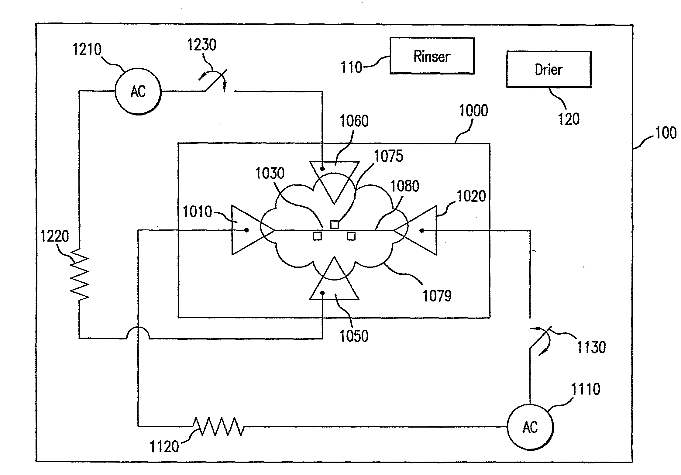
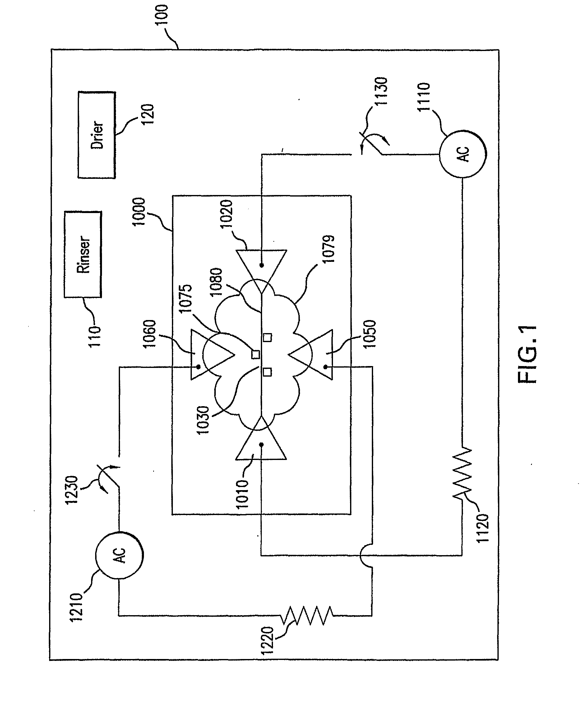
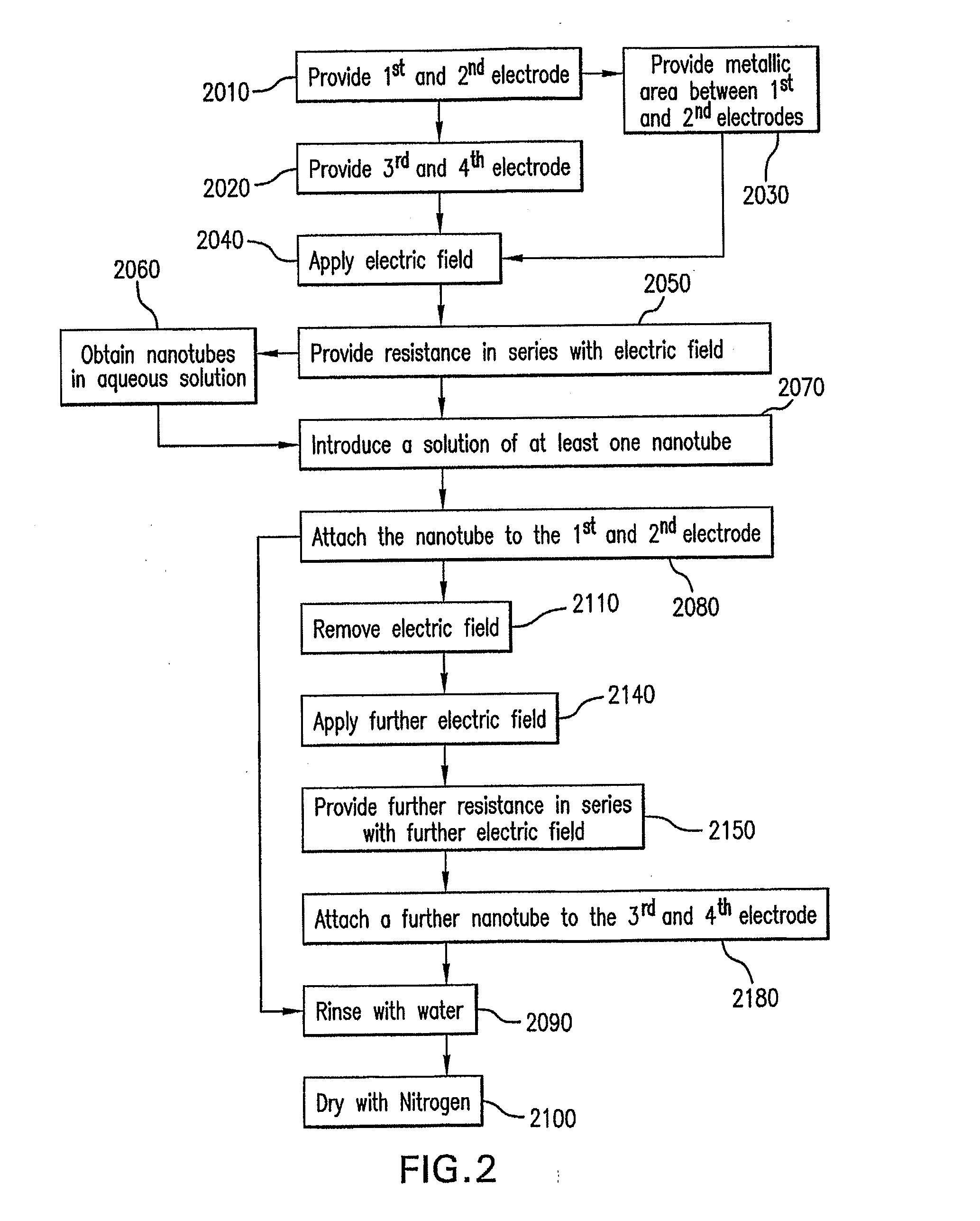
[0054]FIG. 1 is a block diagram of the components of a system according to one exemplary embodiment of the present invention. The system includes a base 100 for receiving a substrate 1000. The substrate 1000 may be formed of SiO2 (500 nanometer) / Si. Any gate dielectric surface may be used instead of SiO2, examples include 1) silicon nitride Si3N4 2) hafnia HfO2, 3) zirconia ZrO2, 4) alumina Al2O3, 5) glass, or 6) plastic. The thicknesses can range from 5 nanometer to 1 micrometer. Alternatives for silicon include indium tin oxide (ITO) or any metallic surface. The substrate 1000 includes a first electrode 1010 and a second electrode 1020 which may be patterned thereon by electron beam lithography or optical lithography, followed by thermal or electron beam evaporation of Cr / Au electrodes. Any relatively inert metal electrodes may be used including gold, platinum, palladium, gold-palladium alloys, indium, etc. The thickness of the electrodes may range from 50-250 nanometers. Between ...
PUM
| Property | Measurement | Unit |
|---|---|---|
| Time | aaaaa | aaaaa |
| Frequency | aaaaa | aaaaa |
| Frequency | aaaaa | aaaaa |
Abstract
Description
Claims
Application Information