Drying apparatus with exhaust control cap for semiconductor wafers and associated methods

a drying apparatus and control cap technology, applied in lighting and heating apparatus, machine/engine, cleaning using liquids, etc., can solve the problems of reducing the yield and reliability of the wafer, and achieve the effect of improving the way vapor from the drying section of the drying apparatus is contained and exhausted

Active Publication Date: 2013-08-08
STMICROELECTRONICS SRL
View PDF4 Cites 11 Cited by
  • Summary
  • Abstract
  • Description
  • Claims
  • Application Information

AI Technical Summary

Benefits of technology

[0008]In view of the foregoing background, it is therefore an object of the present invention to improve how vapor from the drying section of a drying apparatus is contained and exhausted.

Problems solved by technology

This will lead to wafer yield and reliability being decreased.
This is particularly so if the rinsing liquid within the rinsing section is toxic.

Method used


Image

  • Drying apparatus with exhaust control cap for semiconductor wafers and associated methods
  • Drying apparatus with exhaust control cap for semiconductor wafers and associated methods
  • Drying apparatus with exhaust control cap for semiconductor wafers and associated methods

Examples


Embodiment Construction

[0031]The present invention will now be described more fully hereinafter with reference to the accompanying drawings, in which preferred embodiments of the invention are shown. This invention may, however, be embodied in many different forms and should not be construed as limited to the embodiments set forth herein. Rather, these embodiments are provided so that this disclosure will be thorough and complete, and will fully convey the scope of the invention to those skilled in the art. Like numbers refer to like elements throughout, and prime and multiple prime notations are used to indicate similar elements in alternative embodiments.

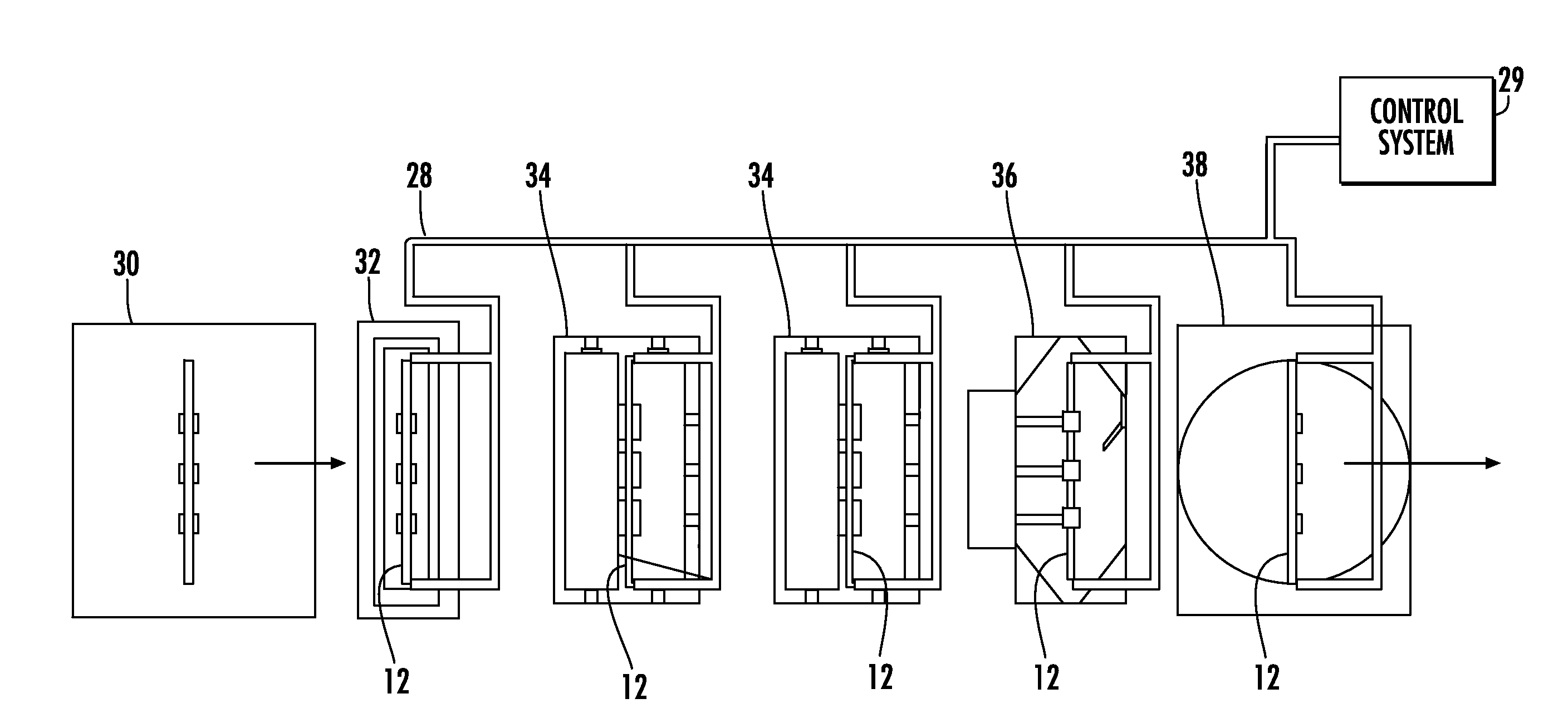
[0032]An overview of post chemical-mechanical polishing (CMP) cleaning stations used to clean semiconductor wafers 12 after CMP will initially be discussed in reference to FIG. 3. Each clean station represents one or more steps in the post CMP wafer buffing and cleaning process. For maximum throughput, at least one semiconductor wafer 12 is simultaneous...


PUM

PropertyMeasurementUnit
frequencyaaaaaaaaaa
frequencyaaaaaaaaaa
abrasiveaaaaaaaaaa

Abstract

A drying apparatus for drying a semiconductor wafer includes a processing chamber including a rinsing section and a drying section adjacent thereto. The rinsing section has a chamber loading slot associated therewith for receiving the semiconductor wafer. The drying section has a chamber unloading slot associated therewith for outputting the semiconductor wafer. An exhaust control cap is carried by the processing chamber and includes a bottom wall, a top wall, at least one intermediate wall between the bottom and top walls, and a side wall coupled to the top, bottom and the at least one intermediate wall to define stacked exhaust sections. The exhaust control cap has a cap loading slot aligned with the chamber loading slot, a cap unloading slot aligned with the chamber unloading slot, and at least one exhaust port configured to be coupled to a vacuum source.

Description

FIELD OF THE INVENTION[0001]The present invention relates to the field of semiconductor wafers, and more particularly, to an apparatus and method for rinsing and drying semiconductor wafers.BACKGROUND OF THE INVENTION[0002]Chemical-mechanical polishing (CMP) is performed in the processing of semiconductor wafers. A standard CMP apparatus has a circular polishing pad and a rotating carrier for holding a semiconductor wafer. An abrasive slurry is used on the polishing pad. After a CMP operation, residual particles are left on the surface of the semiconductor wafer. These residual particles need to be removed.[0003]Semiconductor wafers are typically cleaned in a cleaning apparatus which includes one or more brush stations each having a pair of rotary brushes for cleaning the major surfaces of the wafers. A conventional cleaning apparatus 10 is illustrated in FIG. 1. The cleaning apparatus 10 includes a pair of brushes 12 that clean the major surfaces of a semiconductor wafer 14 placed ...

Claims


Application Information

Patent Timeline
Patent Type & Authority Applications(United States)
IPC IPC(8): B08B3/00B23P17/00F03B11/02
CPCA46B13/02B08B1/04F26B21/00Y10T29/494H01L21/67046A46B13/001H01L21/67034Y10T137/8593
Inventor ZHANG, JOHN H.
Owner STMICROELECTRONICS SRL
Why Eureka
Try Eureka