Solid state illumination device having plasmonic antenna array for anisotropic emission

Active Publication Date: 2016-06-09
LUMILEDS
View PDF4 Cites 36 Cited by
  • Summary
  • Abstract
  • Description
  • Claims
  • Application Information

AI Technical Summary

Benefits of technology

[0017]A particular advantage of the present invention is that by arranging the photon emitter such that the spatial extension of the hybrid coupled LSPR and photonic modes of the plasmonic antenna array overlaps the photon emitter, coupling between the emitted photon and the plasmonic antenna array occur such that the direction of the emitted photon is controlled by the plasmonic antenna array in the same manner as discussed above.
[0018]Accordingly, for a photon emitter arranged such that coupling occurs between the photon emitter and the plasmonic antenna array, an emitted photon may be seen as being emitted from the coupled system comprising the photon emitter and plasmon antenna array. In general, the photon emitter in an excited state may either emit a photon directly, or through coupled emission where coupling occurs between the photon emitter and modes of the plasmonic antenna array.
[0019]In applications where an ensemble of photon emitters is used, and where the individual photon emitters have different emission wavelengths, the plasmonic antenna array may be configured such that the directionality of a particular wavelength is enhanced, thereby making it possible to also control the resulting spectra being emitted from the illumination device, at least for the particular emission angle range determined by the antenna array

Problems solved by technology

This means that blue light will also be scattered back into the diode which leads to absorption losses in the LED.
This leads to further losses as only a portion of the light escapes through the output surface of the light emitting device.
However, to be able to control the emission direction, a photonic band gap material needs to be made from materials having a high refractive index contrast, high aspect ratio holes or pillars must be patterned and

Method used


Image

  • Solid state illumination device having plasmonic antenna array for anisotropic emission
  • Solid state illumination device having plasmonic antenna array for anisotropic emission
  • Solid state illumination device having plasmonic antenna array for anisotropic emission

Examples


Embodiment Construction

[0059]The present invention will now be described more fully hereinafter with reference to the accompanying drawings, in which exemplary embodiments of the invention are shown. This invention may, however, be embodied in many different forms and should not be construed as limited to the embodiments set forth herein; rather, these embodiments are provided for thoroughness and completeness, and fully convey the scope of the invention to the skilled person. Like reference characters refer to like elements throughout.

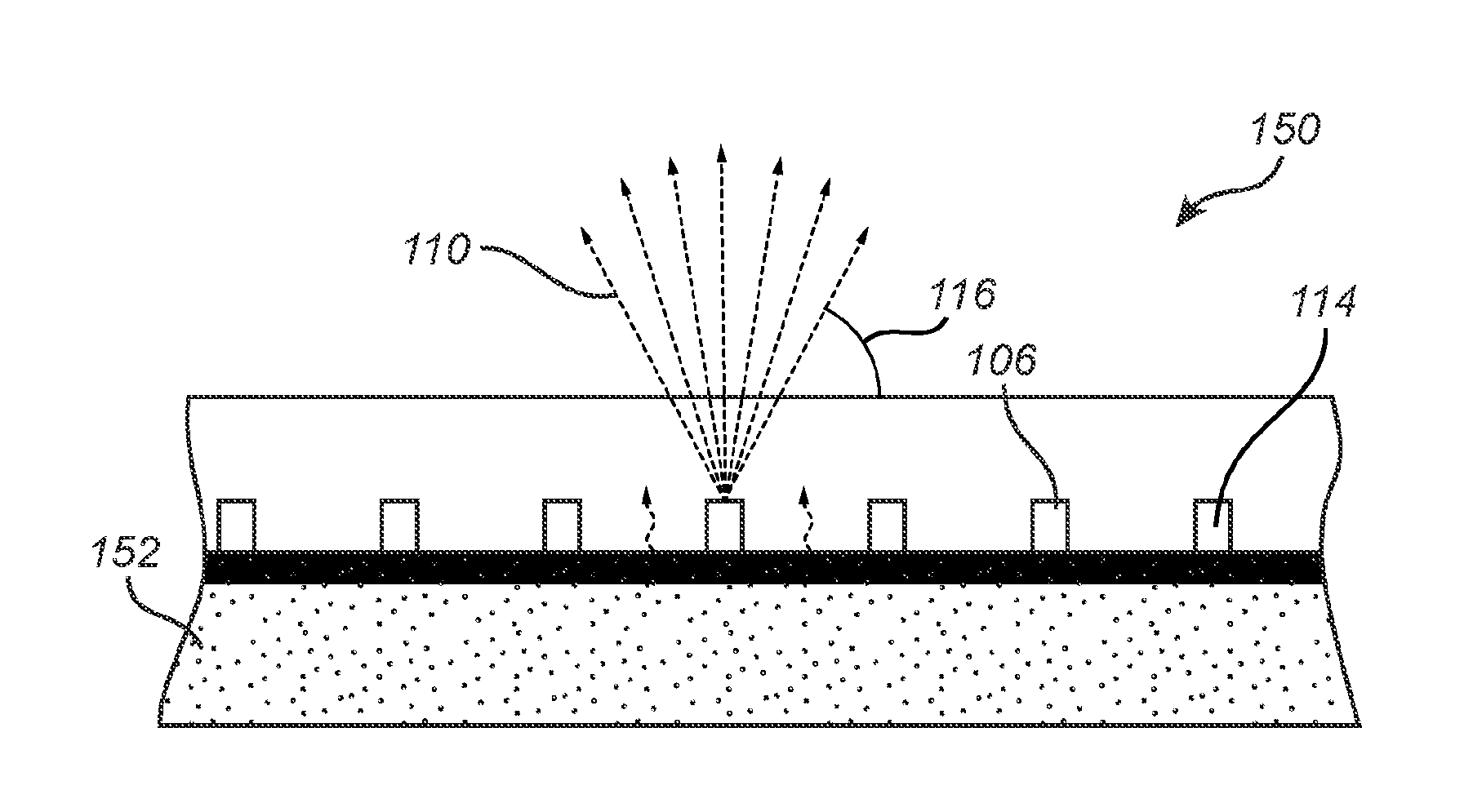
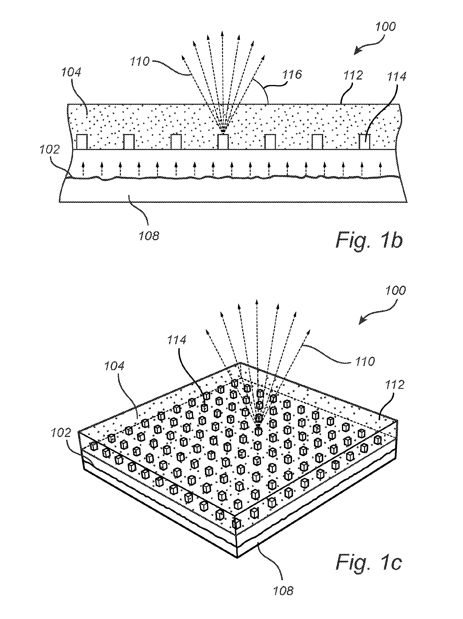
[0060]FIG. 1a is a schematic illustration of an illumination device 150 comprising a plurality of photon emitters 152 arranged in close proximity to a periodic plasmonic antenna array 114 comprising a plurality of individual antenna elements 106 arranged in an antenna array plane as illustrated by FIG. 1c. The antenna array 114 is here arranged on a substrate 108, which is illustrated to comprise the photon emitter 102.

[0061]The distance between the photon emitter and one o...


PUM


Abstract

There is provided an illumination device (100, 150, 200, 300) comprising: a periodic plasmonic antenna array (114), comprising a plurality of individual antenna elements (106) arranged in an antenna array plane, the plasmonic antenna array being configured to support surface lattice resonances at a first wavelength, arising from diffractive coupling of localized surface plasmon resonances in the individual antenna elements; a photon emitter (152) configured to emit photons at the first wavelength, the photon emitter being arranged in close proximity of the plasmonic antenna array such that at least a portion of the emitted photons are emitted by a coupled system comprising said photon emitter and said plasmonic antenna array, wherein the plasmonic antenna array is configured to comprise plasmon resonance modes being out-of plane asymmetric, such that light emitted from the plasmonic antenna array has an anisotropic angle distribution.

Description

FIELD OF THE INVENTION[0001]The present invention relates to an illumination device. In particular, the present invention related to an illumination device having improved emission properties.TECHNICAL BACKGROUND[0002]For light emitting diodes (LEDs) for use in lighting applications, it is desirable to provide essentially white light having a color temperature approximately comparable to that produced by incandescent lighting.[0003]White light from LEDs is commonly provided by using a pn-diode emitting blue light, having a wavelength around 450 nm, where part of the blue light is converted to longer wavelengths using one or more wavelength converting materials arranged on top of or in the vicinity of the diode. By combining the converted light with the unabsorbed blue light, a reasonably broadband spectrum which is perceived as white light can be obtained.[0004]Currently, in most commercial applications, the wavelength converting material is applied directly on the LED. Furthermore,...

Claims


Application Information

Patent Timeline
IPC IPC(8): G02B5/00H01S5/00H01L33/50
CPCG02B5/008H01S5/005H01L33/508H01L33/58
Inventor VERSCHUUREN, MARCUS ANTONIUSRAHIMZADEH KALALEH RODRIGUEZ, SAIDLOZANO BARBERO, GABRIEL SEBASTIANMURAI, SUNSUKEGOMEZ RIVAS, JAIMELOUWERS, DAVYDE BOER, DIRK KORNELIS GERHARDUSIVAN, MARIUS GABRIELHIKMET, RIFAT ATA MUSTAFAVAN BOMMEL, TIES
Owner LUMILEDS
Why Eureka
Try Eureka