


Quick Research
Generate reliable direction feasibility study reports for your R&D in just a few steps.

Technical Q&A
Discover and master advanced knowledge NOW. Basics, ideas, possibilities, all at once.

Find Solutions
As an expert in R&D theories, this can generate solutions to your technical problems instantly.

Evaluate Feasibility
Analyze your overall solution with one click, know your potential R&D risks in advance.

Monitor Landscape
Get weekly tech updates, stay abreast of the latest tech innovations and key insights.
Organic electroluminescent element
a technology of electroluminescent elements and organic materials, applied in the direction of organic semiconductor devices, luminescent compositions, thermoelectric devices, etc., can solve the problems of low luminescence efficiency of white luminescent panels for illumination, ineffective use of most of the light, and inability to achieve high efficiency and long life of white luminescent panels, etc., to achieve suppressed deterioration of luminance and drive voltage rise, and suppressed occurrence of luminance unevenness
- Summary
- Abstract
- Description
- Claims
- Application Information
AI Technical Summary
Benefits of technology
Problems solved by technology
Method used
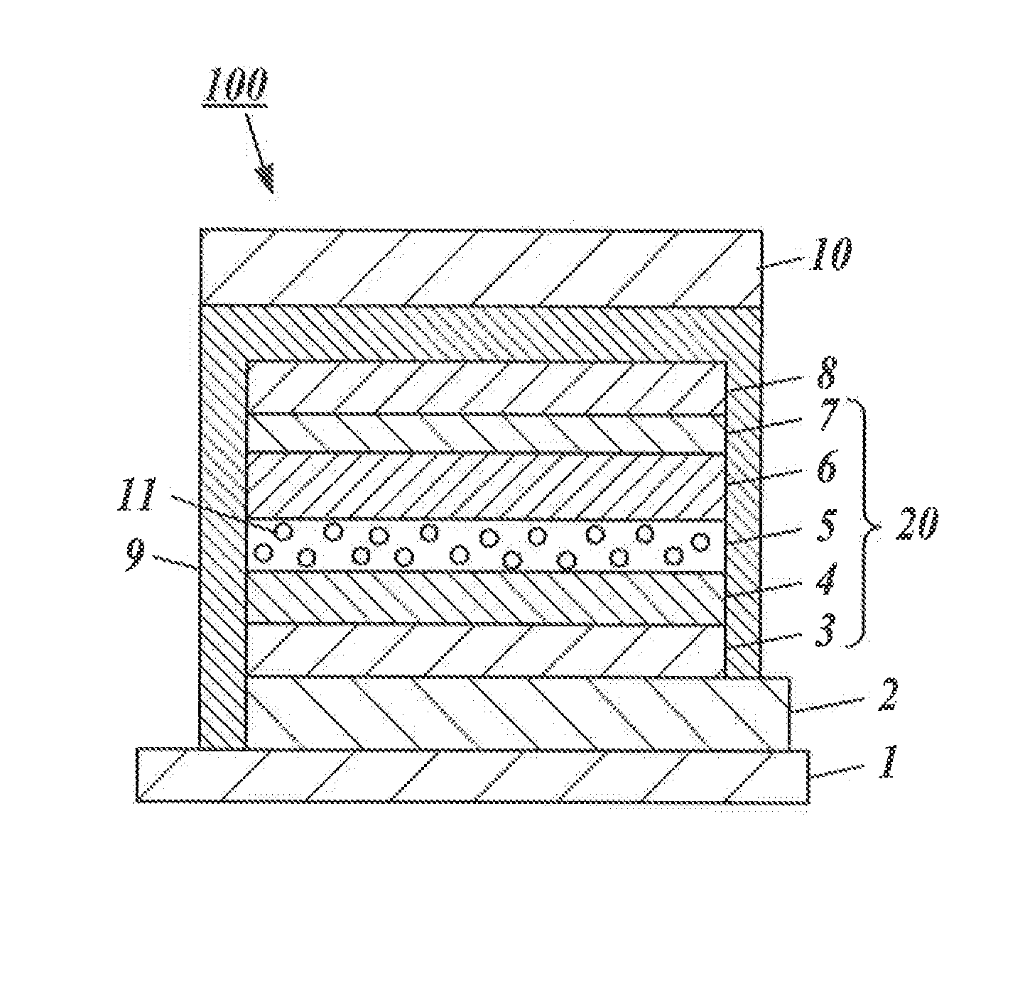
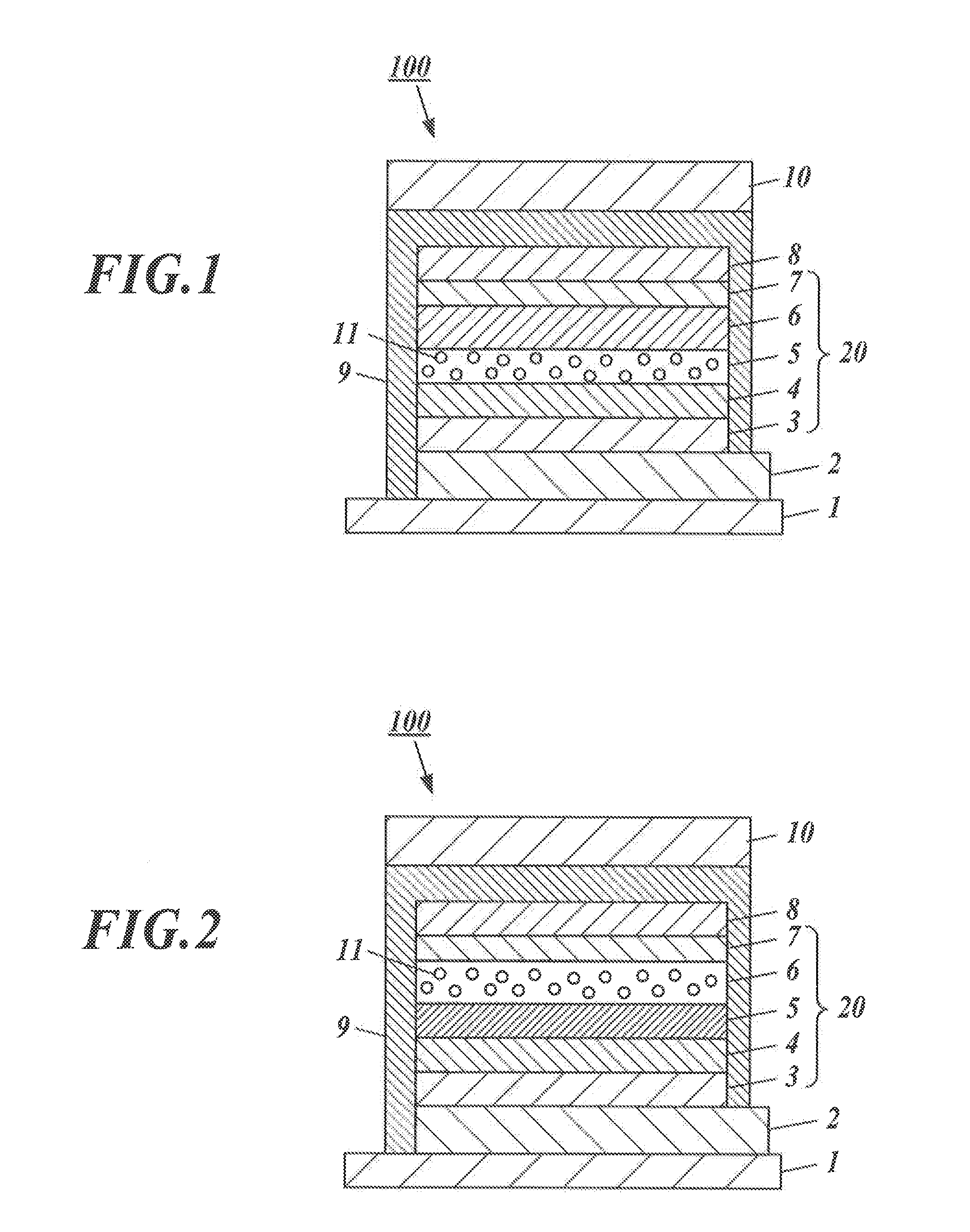
Image

Examples
embodiment
[0237]Hereinafter, the present invention will be explained with reference to embodiments. However, the present invention is not limited thereto. Note that “part” and “%” used in the embodiment respectively represents “parts by weight” and “percent by weight.”
[0238]>
[0239](1) Manufacturing of Samples 100 to 108
[0240](1.1) Manufacturing of Gas Barrier Flexible Film
[0241]On the entire surface a polyethylene naphthalete film (a film which is a product of Teijin Dupont Films Japan Limited, hereinafter abbreviated as PEN) where a first electrode was to be formed, inorganic gas-barrier films including SiOx were formed continuously by use of an atmospheric-pressure plasma discharge treatment device having a configuration described in the Japanese Unexamined Patent Application Publication No. 2004-68143 to have a thickness of 500 nm to manufacture a gas-barrier flexible film having the oxygen permeability equal to or less than 0.001 ml / m2 / day and the water vapor permeability of equal to or l...
PUM
 Abstract
Description
Claims
Application Information
 - R&D Engineer
- R&D Manager
- IP Professional
- Industry Leading Data Capabilities
- Powerful AI technology
- Patent DNA Extraction
Browse by: Latest US Patents, China's latest patents, Technical Efficacy Thesaurus, Application Domain, Technology Topic, Popular Technical Reports.
© 2024 PatSnap. All rights reserved.Legal|Privacy policy|Modern Slavery Act Transparency Statement|Sitemap|About US| Contact US: help@patsnap.com