Chip assembly system

a chip assembly and integrated circuit technology, applied in the direction of semiconductor devices, semiconductor/solid-state device details, electrical apparatus, etc., can solve the problems of affecting the operation of the electronic components formed, difficulty in avoiding, and lack of reliability of the obtained components

Active Publication Date: 2013-08-15
STMICROELECTRONICS (CROLLES 2) SAS
View PDF2 Cites 51 Cited by
  • Summary
  • Abstract
  • Description
  • Claims
  • Application Information

AI Technical Summary

Problems solved by technology

However, as illustrated in FIG. 3, this type of assembly has a disadvantage in the case where there is a misalignment between opposite pads Pi1 and Pi2 at the time of the assembly, which is difficult to avoid in practice.
A lack of reliability of the obtained components can then be observed during their lifetime.
This lack of reliability i

Method used


Image

  • Chip assembly system
  • Chip assembly system
  • Chip assembly system

Examples


Embodiment Construction

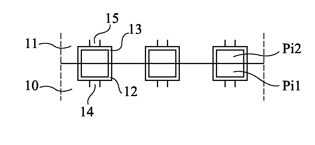
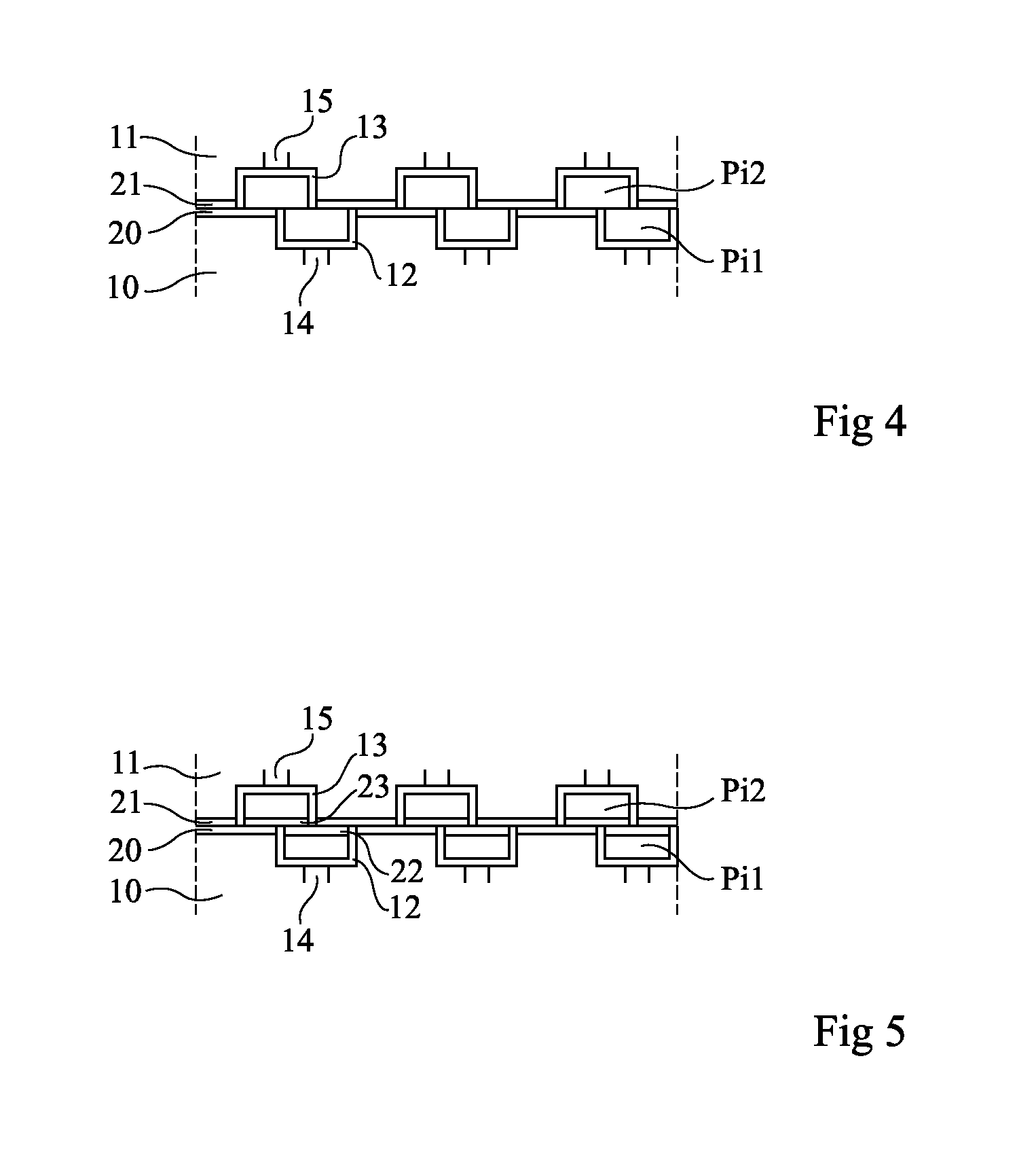
[0023]FIG. 4 shows the external surfaces of an assembly according to the present invention. It shows the same pads Pi1, Pi2 as those described and shown in relation with FIGS. 2 and 3.

[0024]In this embodiment, the pads are now formed in a silicon oxide layer covered with an insulating layer 20, 21 of a material haying, on the one hand, like silicon oxide, the advantage that the two opposite polished surfaces bond to each other by molecular bonding and, on the other hand, the advantage that copper is not capable of diffusing therein. A preferred example of such a material is silicon nitride (Si3N4) or SiCN.

[0025]FIG. 5 shows another variation of the assembly of FIG. 4. The same elements are designated with the same reference numerals in FIG. 4. In this embodiment, a thin barrier layer 22, 23 of a copper silicon nitride CuSiN self positioned on the external surface of the copper pads is formed by successively or simultaneously performing a siliciding and a nitriding of the external su...


PUM


Abstract

An assembly of semiconductor wafers/chips wherein the adjacent surfaces of the two wafers/chips comprise an insulating layer having opposite copper pads inserted therein. The insulating layer is made of a material selected from the group including silicon nitride and silicon carbon nitride.

Description

CROSS REFERENCE TO RELATED APPLICATION[0001]This application is a translation of and claims the priority benefit of French patent application number 12 / 51362, filed on Feb. 14, 2012, entitled “CHIP ASSEMBLY SYSTEM,” which is hereby incorporated by reference to the maximum extent allowable by law.BACKGROUND[0002]The present disclosure relates to the field of three-dimensional integrated circuits. Indeed, to increase the integration level of semiconductor components, there is a tendency to form integrated circuits made of a stack of chips.[0003]FIGS. 1A and 1B very schematically show a three-dimensional assembly of semiconductor components. A first semiconductor element (chip or wafer) W1 supports a second semiconductor element W2 (a wafer or one or several second semiconductor wafers). The opposite surfaces of each of semiconductor elements W1, W2 are coated with an interconnection structure, respectively I1, I2. Each of interconnection structures I1, I2 comprises a number of metalli...

Claims


Application Information

Patent Timeline
IPC IPC(8): H01L23/492
CPCH01L2224/06517H01L2225/06513H01L2224/80357H01L2224/08147H01L24/05H01L24/06H01L24/08H01L24/80H01L25/0657H01L2224/05647H01L2224/05657H01L2224/05687H01L2224/08145H01L2224/80097H01L2224/05688H01L25/50H01L2224/08121H01L2224/05547H01L23/4924H01L2924/01014H01L2924/01007H01L2924/01074H01L2924/01015H01L2924/05042H01L2924/04642H01L2924/059H01L2924/049H01L2224/80895H01L2224/80896H01L2224/8034H01L2224/09517H01L2224/80359
Inventor CHAPELON, LAURENT-LUC
Owner STMICROELECTRONICS (CROLLES 2) SAS
Why Eureka
Try Eureka