Device module

a technology of device modules and modules, applied in the field of device modules, can solve the problems of poor yield rate of device modules, and achieve the effects of improving the adhesiveness of the reinforcing part, reducing the amount of plastic materials, and reducing the possibility of leakage of some plastic materials

Active Publication Date: 2013-08-15
HOSIDEN CORP
View PDF15 Cites 1 Cited by
  • Summary
  • Abstract
  • Description
  • Claims
  • Application Information

AI Technical Summary

Benefits of technology

[0008]A device module in accordance with an aspect of the invention includes a device, a connecting part, and a plastic part. The device is a sensor, an electronic component, or a circuit board. The connecting part is connected to the device and includes an external connecting portion. The device and the connecting part are embedded in the plastic part. The plastic part is provided with a first opening that exposes at least the external connecting portion of the connecting part to the outside. This aspect of the invention makes it possible to obviate a step of fixing the device to the plastic part because the device is embedded in the plastic part. This should lead to increased yield rate of the device module. Moreover, the device embedded in the plastic part is connected to the connecting part, and the external connecting portion of the connecting part is exposed from the first opening of the plastic part. Such external connecting portion facilitates external connection of the device.
[0019]The plastic part may further include a second opening provided on an opposite side of the device from the sheet. In this aspect of the invention, the plastic part provided with the second opening can be fabricated with reduced amount of plastic material, leading to reduced cost of the device module. Moreover, as the device is embedded below the second opening of the plastic part, it is possible to compensate reduction in strength of the plastic part due to reduced thickness of the plastic part by providing the second opening.

Problems solved by technology

Unfortunately, the ribbed parts interfere with attaching the sensor to the back face of the plastic part, which may lead to poor yield rate of the device module.

Method used


Image

  • Device module
  • Device module
  • Device module

Examples


first embodiment

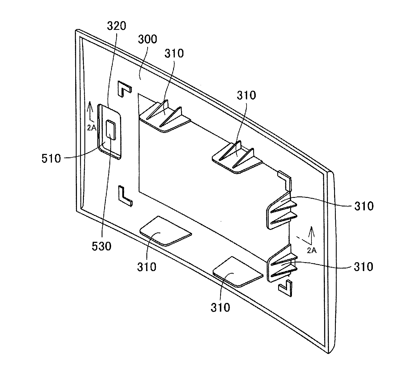
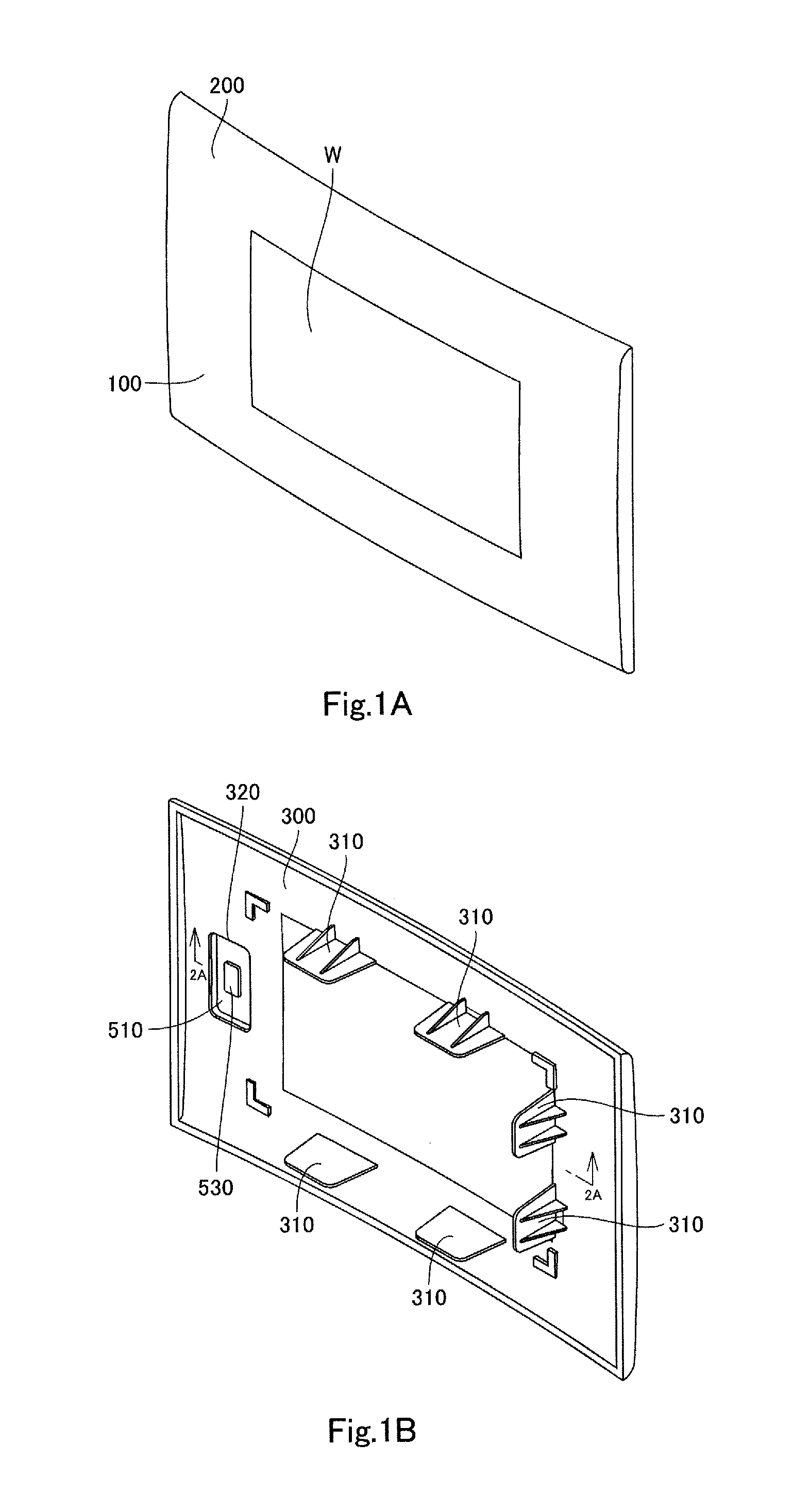
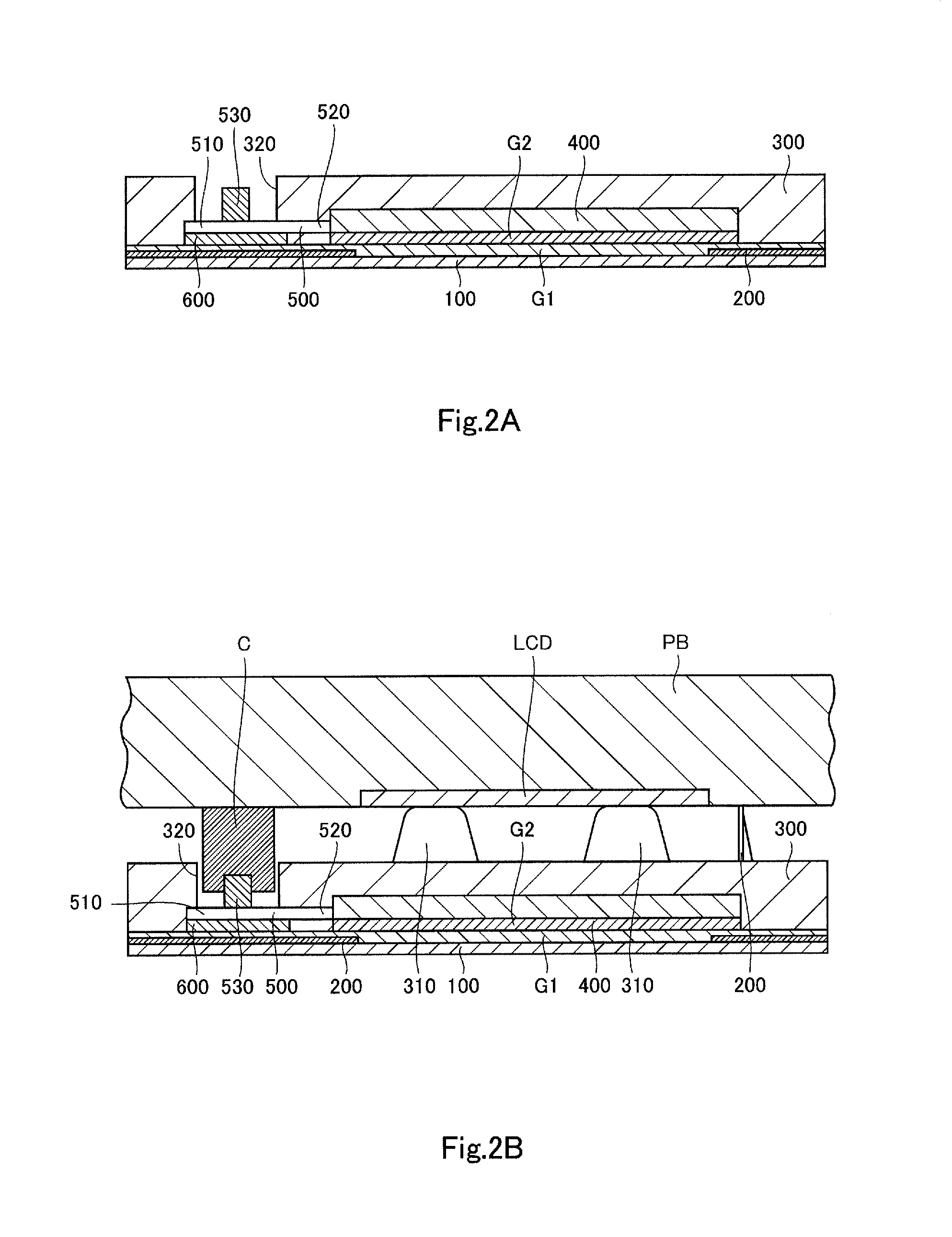
[0047]First, a device module in accordance with the First embodiment will be described with reference to FIG. 1A to FIG. 2B. The device module shown in FIG. 1A to FIG. 2B is a touch sensing device. The device module includes a sheet 100, an ornamental layer 200, a plastic part 300, a touch sensor 400 (corresponding to the device in the claims), a connecting part 500, and a reinforcing part 600. These constituents of the device module will be described below in detail.

[0048]The sheet 100 is a substantially rectangular flexible film of optically transparent resin such as PET (polyethylene terephthalate) and acrylic resin. The sheet 100 has an outer face and an inner face (the lower and upper faces in FIG. 2A and FIG. 2B). As shown in FIG. 1A and FIG. 1B, the periphery of the inner face of the sheet 100 is subjected to ornamental printing (e.g. painted in black) in a flame shape to form the ornamental layer 200. The ornamental layer 200 defines a rectangular transparent window W in the...

second embodiment

[0068]Next, a device module in accordance with Second embodiment will be described with reference to FIG. 3 and FIG. 4. The device module shown in FIG. 3 has substantially the same configuration as that of the First embodiment and differs only in having a plurality of external connecting portions 530′ on a first end 510′ of a connecting part 500′, and a plurality of first openings 320′ to expose only the external connecting portions 530′ from the plastic part 300′. Only these differences will be described below in detail, and redundant description will be omitted. A symbol _′_ is added to the reference numerals of the plastic part and the connecting part and their subcomponents to distinguish them from those of the First embodiment.

[0069]The external connecting portions 530′, which may be contacts or electrodes, are provided on the first end 510′ of the connecting part 500′. The plurality of first openings 320′ are columnar and formed in the plastic part 300′. The first openings 320...

third embodiment

[0074]A device module in accordance with the Third embodiment will be described with reference to FIG. 5A and FIG. 5B. The device module shown in FIG. 5A and FIG. 5B has substantially the same configuration as the device module of the First embodiment and differs only in having an engaging part 700 in place of the reinforcing part 600, a first end 510″ of a connecting part 500″ serving as an external connecting portion, and an about half of the connecting part 500′ on the first end 510″ side led out from a first opening 320″ of a plastic part 300″. Only these differences will be described below in detail, and redundant description will be omitted. A symbol _″_ is added to the reference numerals of the plastic part and the connecting part and their subcomponents to distinguish them from those of the First embodiment. A symbol _′_ is added to the reference numeral of the sheet to distinguish it from that of the First embodiment.

[0075]The engaging part 700 is a block having a substanti...


PUM


Abstract

The invention provides a device module including a device, a connecting part, and a plastic part. The device is a sensor, an electronic component, or a circuit board. The connecting part is connected to the device and includes an external connecting portion. The device and the connecting part are embedded in the plastic part. The plastic part is provided with a first opening that exposes at least the external connecting portion of the connecting part to the outside.

Description

[0001]The present application claims priority under 35 U.S.C. §119 of Japanese Patent Application No. 2012-27108 filed on Feb. 10, 2012, the disclosure of which is expressly incorporated by reference herein in its entity.BACKGROUND OF THE INVENTION[0002]1. Technical Field[0003]The invention relates to device modules.[0004]2. Background Art[0005]There is a known device module including an ornamental panel as disclosed in Japanese Unexamined Patent Application Publication No. 2006-281601 and a sensor such as a touch panel. The ornamental panel includes a transparent sheet that is touchable by an object to be detected such as a finger, a plastic part disposed on the sheet, and an ornamental layer provided between the sheet and the plastic part. The sensor is fixed to a back face of the plastic part.SUMMARY OF INVENTION[0006]The known device module is provided on the back face of plastic part with ribbed parts for attaching the ornamental panel to electronic equipment. Unfortunately, th...

Claims


Application Information

Patent Timeline
Patent Type & Authority Applications(United States)
IPC IPC(8): H05K7/00
CPCH05K7/00H05K5/0017G06F1/1626G06F3/041H03K2217/960785G06F3/044H03K17/962H03K2217/96031H03K2217/960755G06F2203/04103G06F3/0445H04R1/1033H01B7/08B65H75/406H02G11/02
Inventor SHINODA, KOJIISODA, TAKESHI
Owner HOSIDEN CORP
Why Eureka
Try Eureka