
Laminate and method for separating the same

Active Publication Date: 2013-08-29
TOKYO OHKA KOGYO CO LTD
View PDF6 Cites 5 Cited by
  • Summary
  • Abstract
  • Description
  • Claims
  • Application Information

AI Technical Summary

Benefits of technology

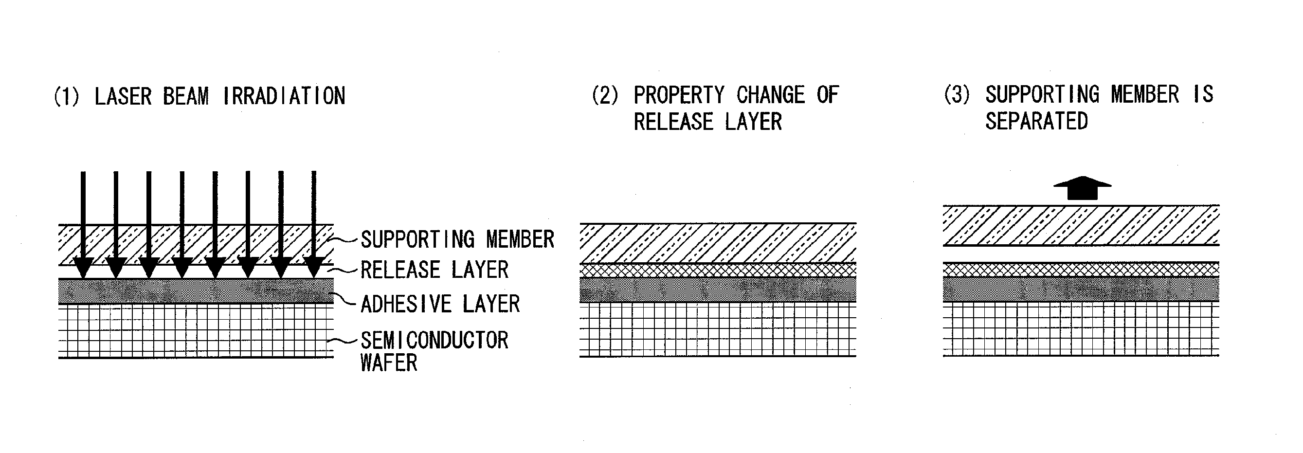
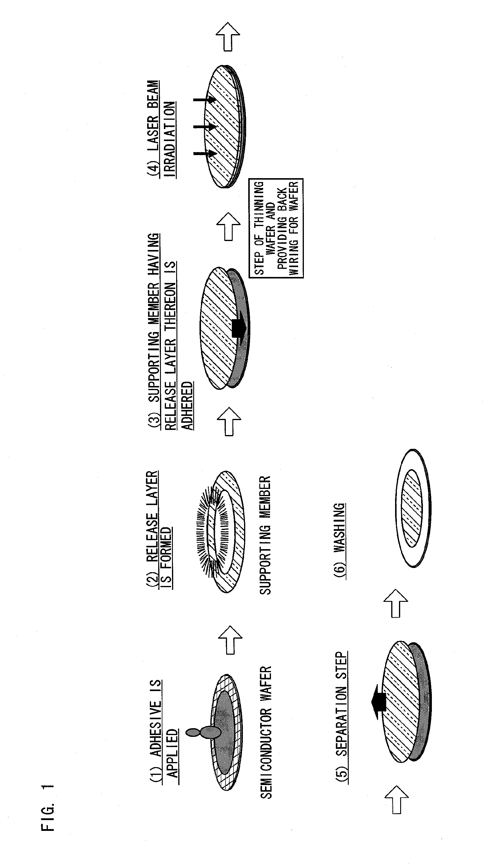
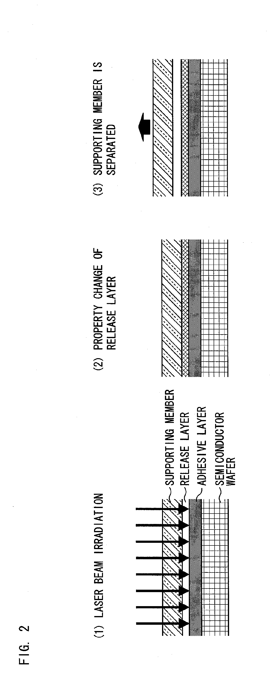
The present invention allows for the creation of a lamination where a target object is firmly attached to a supporting member, but the supporting member can easily be separated from the target object. The invention also provides a method for separating the lamination.

Problems solved by technology

This is likely to result in a crack or a warpage in the wafer.
Furthermore, it is difficult to automatically carry the wafer whose strength decreases due to its smaller thickness.
Therefore, it is necessary to manually carry the wafer and it is troublesome to handle the wafer.

Method used


Image

  • Laminate and method for separating the same
  • Laminate and method for separating the same
  • Laminate and method for separating the same

Examples


example 1

Production of Laminate

[0053]A laminate in accordance with Example 1 was produced in the following manner. In a plasma CVD device, a CHF3 gas was used to form a fluorocarbon film on a plate-like supporting member having a thickness of 0.7 mm. In this way, a supporting member on which a release layer having a thickness of 1 μm was formed was obtained.

[0054]Next, on a semiconductor wafer substrate (an unground silicon wafer having a diameter of 150 mm) having a thickness of 725 μm, a hydrocarbon adhesive “TZNR-A3007” (manufactured by TOKYO OHKA KOGYO Co., Ltd.) was applied so that the thickness of the hydrocarbon adhesive after baking would be 50 μm. Then, the hydrocarbon adhesive was baked in stages at 90° C., 160° C. and 220° C. for 10 minutes to 20 minutes each, thereby forming an adhesive layer on the semiconductor wafer substrate. Then, the release layer and the adhesive layer were placed against each other and adhered together, thereby obtaining the laminate.

[0055](Evaluation of ...

example 2

[0060]The same processes as in Example 1 were carried out except that a CHF3 gas was replaced with a C4F8 gas, and whether or not the supporting member was separable from the semiconductor wafer substrate was evaluated.

[0061]As a result, also in Example 2, as is the case with Example 1, it was possible to very easily separate the supported substrate from the supporting member by changing a property of the release layer by laser irradiation.


PUM


Abstract

A laminate including a supporting member which is light transmissive; a supported substrate supported by the supporting member; an adhesive layer provided on a surface of the supported substrate which surface faces toward the supporting member; and a release layer which is made of a fluorocarbon and is provided between the supporting member and the supported substrate, the release layer having a property that changes when it absorbs light coming through the supporting member.

Description

TECHNICAL FIELD[0001]The present invention relates to (i) a laminate produced by adhering together a supporting member and a supported substrate supported by the supporting member and (ii) a method for separating the laminate.BACKGROUND ART[0002]As mobile phones, digital AV devices, IC cards and the like are highly functionalized, it is more demanded that a semiconductor silicon chip (hereafter referred to as “chip”) be highly integrated in a package by making a mounted chip smaller and thinner. For instance, there is a demand for thinning of an integrated circuit obtained by packaging a plurality of chips, such as CSP (chip size package) and MCP (multi-chip package). In order to fulfill high integration of a chip in a package, it is necessary to thin a chip down to a range of 25 μm to 150 μm.[0003]However, a semiconductor wafer (hereafter referred to as “wafer”) serving as a base of a chip becomes thin by grinding. Therefore, strength of the wafer decreases. This is likely to resul...

Claims


Application Information

Patent Timeline
IPC IPC(8): H01L21/78H01L23/00
CPCH01L21/6835H01L2221/68318H01L2221/68327H01L2221/6834H01L2221/68381B32B7/06Y10T156/1158H01L21/7813H01L23/562H01L2924/0002C03C17/3452H01L2924/00
Inventor INAO, YOSHIHIROFUJII, YASUSHIMATSUSHITA, ATSUSHITAMURA, KOKIKUBO, ATSUSHI
Owner TOKYO OHKA KOGYO CO LTD
Learn More