Semiconductor module and method of manufacturing a semiconductor module

a semiconductor module and semiconductor technology, applied in the direction of manufacturing tools, non-electric welding apparatus, soldering equipment, etc., can solve the problems of limited reliability of solder connection between terminal and substrate, limited lifetime of the whole semiconductor module, and failure to meet the requirements of the semiconductor modul

Inactive Publication Date: 2013-08-29
ABB RES LTD
View PDF9 Cites 9 Cited by
  • Summary
  • Abstract
  • Description
  • Claims
  • Application Information

AI Technical Summary

Benefits of technology

[0046]According to an exemplary embodiment of the disclosure, the contact element is thus placed on the metallic layer by the deepening. This leads to the advantages like described above with respect to the semiconductor module according to an exemplary embodiment of the disclosure.
[0047]The contact element can be connected to the metallic layer by an ultrasonic welding process. A semiconductor module manufactured according to the disclosure does thus not exhibit disadvantages related to cycling. With respect to an exemplary embodiment of the present disclosure, cycling means an influence of periodically changing conditions, such as with respect to temperature and / or mechanical influence. This as well improves the reliability properties of a semiconductor module according to the disclosure.
[0048]The reliability of a semiconductor module according to an exemplary embodiment of the disclosure can be further improved by the fact that a welding connection can sustain temperatures of 200° C. or more. This additionally makes a semiconductor module manufactured according to the method according to an exemplary embodiment of the disclosure suitable even for high power applications.
[0049]Additionally, a semiconductor module can be manufactured according an exemplary embodiment without the specification of consumables like solder or bond wires. Furthermore, the manufacturing process can be performed without further plating or additional cleaning steps. This can lead to the advantage that the method according to an exemplary embodiment to the disclosure is advantageous with respect to the environmental point of view. Additionally, traditional working steps can be omitted making the method according to the exemplary embodiment of the disclosure time saving and thus cost saving.
[0050]By welding the contact element to the metallic layer, furthermore a highly conductive connection is formed. This makes the semiconductor module according to an exemplary embodiment of the disclosure being suitable for high power applications in which high amounts of electric currents have to be conducted through this connection. Consequently, the semiconductor module according to an exemplary embodiment of the disclosure can include a high power semiconductor module.

Problems solved by technology

A drawback of the known soldering technique is a limited reliability under thermal and mechanical cycling of the soldered connection between terminal and substrate.
Therefore, the connection and thus the whole semiconductor module can have a limited lifetime.
Furthermore, soldered connections can only withstand limited operation temperatures.
Consequently, there can be the risk of the contact element to move in the horizontal plane.
This can lead to the disadvantage that the position in which the contact element is welded may not be the intended position.
Therefore, the formed semiconductor module can be unusable.
Additionally, there is a risk of the contact element to be deformed and hence mechanically weakened while it is moving, or slipping, respectively.
This, again, can lead to the disadvantage of the formed semiconductor module being unusable.
Furthermore, the welding process becomes irreproducible.
This, however, can lead to damages of the contact region where the contact element is welded to, or to the contact element itself.
Such a holding and positioning element, however, can lead to the process becoming more complex and thus the necessity of rather complex apparatus specifications.

Method used


Image

  • Semiconductor module and method of manufacturing a semiconductor module
  • Semiconductor module and method of manufacturing a semiconductor module
  • Semiconductor module and method of manufacturing a semiconductor module

Examples


Embodiment Construction

[0026]Exemplary embodiments of the present disclosure provide an improved semiconductor module and an improved method of manufacturing a semiconductor module.

[0027]For example, exemplary embodiments of the present disclosure provides a semiconductor module and a method of manufacturing a semiconductor module in which the manufacturing method is easier to perform with higher reproducibility and in which the semiconductor module has an improved reliability.

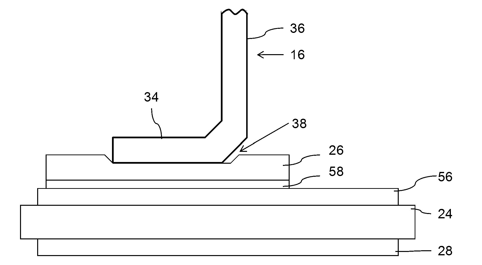
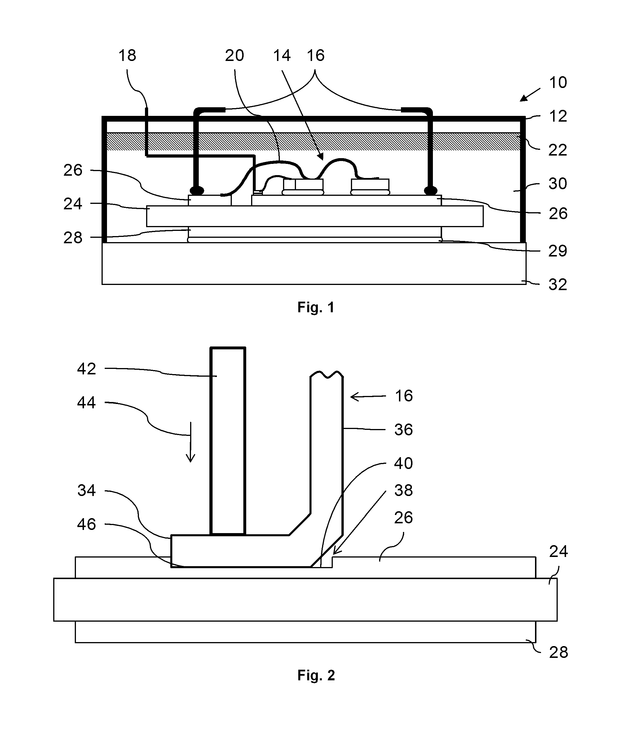
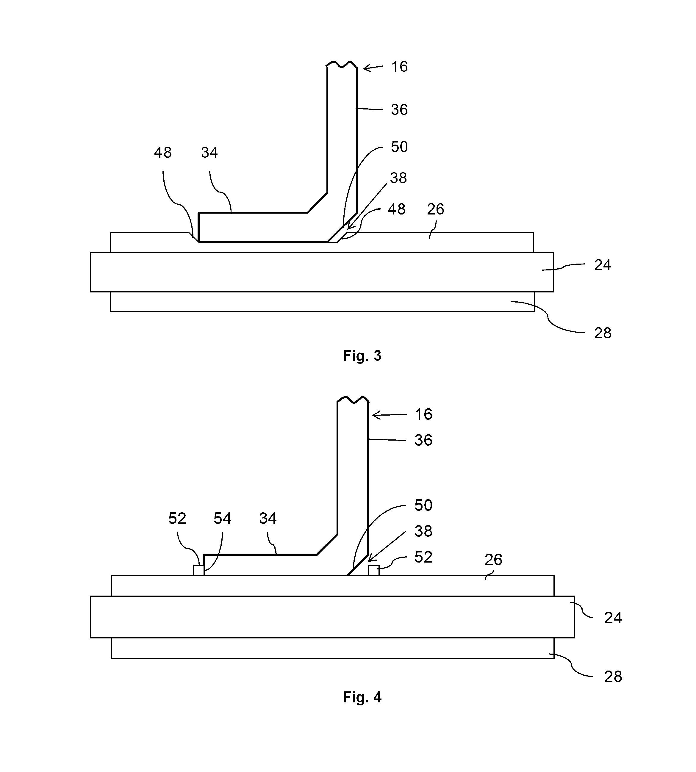
[0028]Exemplary embodiments of the disclosure relate to a semiconductor module, including a substrate, for example, formed of a ceramic insulator, and at least one metallic layer, for example, formed on the substrate, wherein the metallic layer includes a deepening (e.g., a depression) for placing and fixing a contact element, the contact element being at least partially “L”-shaped and including a first arm for fixing the contact element at the deepening, and a second arm for interconnecting the contact element, wherein the deepenin...


PUM

PropertyMeasurementUnit
depthaaaaaaaaaa
temperaturesaaaaaaaaaa

Abstract

An exemplary semiconductor module includes a substrate formed of a ceramic insulator, and at least one metallic layer formed on the substrate. The metallic layer includes a deepening for placing and fixing a contact element. The contact element is at least partially “L”-shaped and includes a first arm for fixing the contact element at the deepening, and a second arm for interconnecting the contact element with an external device. The deepening has a horizontal dimension which is about ≦0.5 mm bigger than the horizontal dimension of the contact element.

Description

RELATED APPLICATION(S)[0001]This application claims priority as a continuation application under 35 U.S.C. §120 to PCT / EP2011 / 067558, which was filed as an International Application on Oct. 7, 2011 designating the U.S., and which claims priority to European Application EP 10187399.0 filed in Europe on Oct. 13, 2010. The content of each prior application is hereby incorporated by reference in its entirety.FIELD[0002]The disclosure relates to a semiconductor module and to a method of manufacturing a semiconductor module.BACKGROUND INFORMATION[0003]A variety of semiconductor modules are known and used in many different electronic devices. For forming or manufacturing a semiconductor module, different electric parts have to be contacted with each other to provide an interlinked internal structure. Additionally, an external contact is provided to connect one or more electric parts of the semiconductor module to an external contact device.[0004]As an example, to achieve an external electr...

Claims


Application Information

Patent Timeline
Patent Type & Authority Applications(United States)
IPC IPC(8): H01L23/495H01L23/00
CPCH01L23/24H01L23/49822H01L2924/1305H01L2924/1306H01L2924/19107H01L24/80H01L23/49517H01L2224/48472H01L2924/01013H05K2203/049H05K2201/09745H05K3/328H05K1/11H01L2924/15787H01L2924/14H01L2924/13091H01L2924/13055H01L2924/1203H01L2924/01079H01L23/49838H01L23/5383H01L23/5386H01L24/32H01L24/45H01L24/48H01L25/072H01L2224/32225H01L2224/45124H01L2224/48091H01L2224/48137H01L2224/48227H01L2224/73265H01L2924/01078H01L2924/00014H01L2924/00012H01L2924/00H01L24/73H01L23/498H01L23/538
Inventor SCHULZ, NICOLAHARTMANN, SAMUEL
Owner ABB RES LTD
Why Eureka
Try Eureka