

Semiconductor device and method of manufacturing the same
- Summary
- Abstract
- Description
- Claims
- Application Information
AI Technical Summary
Benefits of technology
Problems solved by technology
Method used
Image

Examples
first embodiment
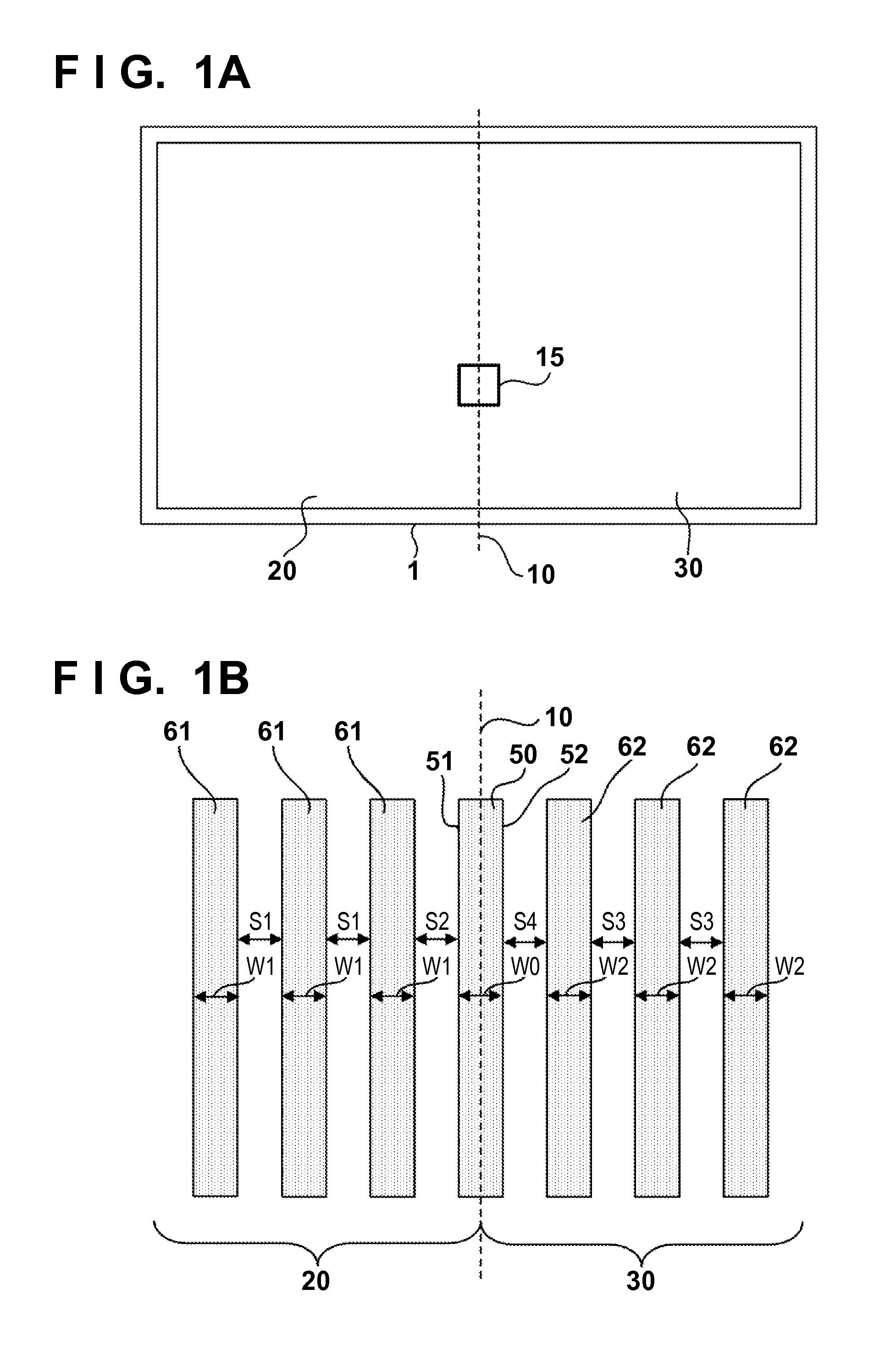
[0022]Therefore, the spaces S1, S2, S3, and S4 between adjacent line portions are independent of the alignment accuracy (excluding the accuracy associated with the projection magnification) in first exposure, and that in second exposure. This means that even if a resist pattern defined in first exposure and that defined in second exposure have shifted from each other, the spaces S1, S2, S3, and S4 between adjacent line portions are independent of the shift. This makes it possible to reduce a variation in capacitance between adjacent line portions, including, for example, line portions in regions near the boundary line 10.
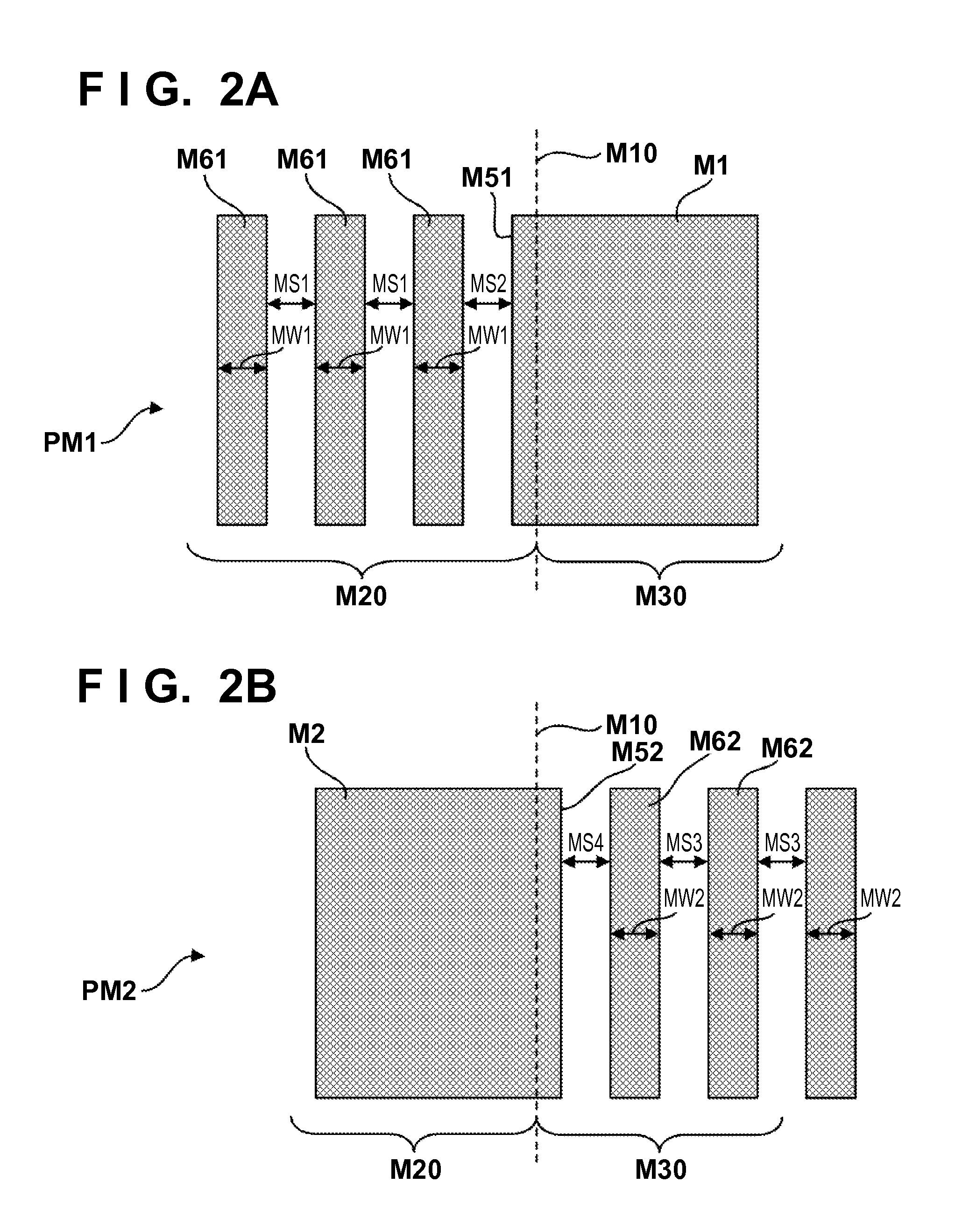
[0023]FIG. 2A illustrates the first photomask PM1 used for first exposure in which the first region 20 is exposed, and FIG. 2B illustrates the second photomask PM2 used for second exposure in which the second region 30 is exposed. Although the case wherein the photoresist used serves as a positive photoresist will be exemplified herein, the present invention is als...
second embodiment
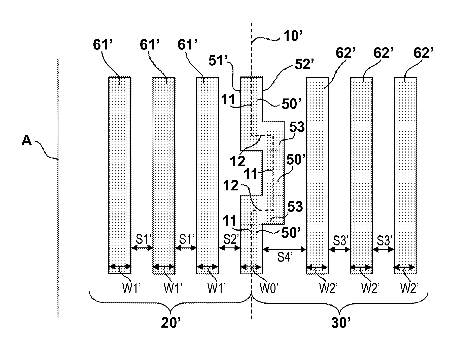
[0031]FIG. 5A is a plan view showing the configuration of a semiconductor device (for example, a semiconductor chip) 1′ according to the present invention. FIG. 5B is an enlarged view of a region including a boundary line 10′ shown in FIG. 5B. FIG. 6A illustrates a first photomask PM1′ used for first exposure in which a first region 20′ is exposed, and FIG. 6B illustrates a second photomask PM2′ used for second exposure in which a second region 30′ is exposed. The semiconductor device 1′ includes, as a plurality of regions, a first region 20′ and second region 30′ which are adjacent to each other on the boundary line 10′. The first region 20′ is exposed using the first photomask PM1′ in a photolithography step for manufacturing the semiconductor device 1′. The second region 30′ is exposed using the second photomask PM2′ in the photolithography step. Note that the first photomask PM1′ and second photomask PM2′ may be formed on different members or in different regions on one member.
[...
PUM
 Abstract
Description
Claims
Application Information