Test IP-Based A.T.E. Instrument Architecture

Inactive Publication Date: 2013-08-29
CZAMARA ALLEN J +2
View PDF16 Cites 31 Cited by
  • Summary
  • Abstract
  • Description
  • Claims
  • Application Information

AI Technical Summary

Benefits of technology

[0033]The present invention provides an improved implementation of automatic testing equipment for semiconductor devices, by providing a Test IP (TIP) b

Problems solved by technology

The fixed instrument architectures must be designed to span a wide range of protocols which result

Method used


Image

  • Test IP-Based A.T.E. Instrument Architecture
  • Test IP-Based A.T.E. Instrument Architecture
  • Test IP-Based A.T.E. Instrument Architecture

Examples


second embodiment

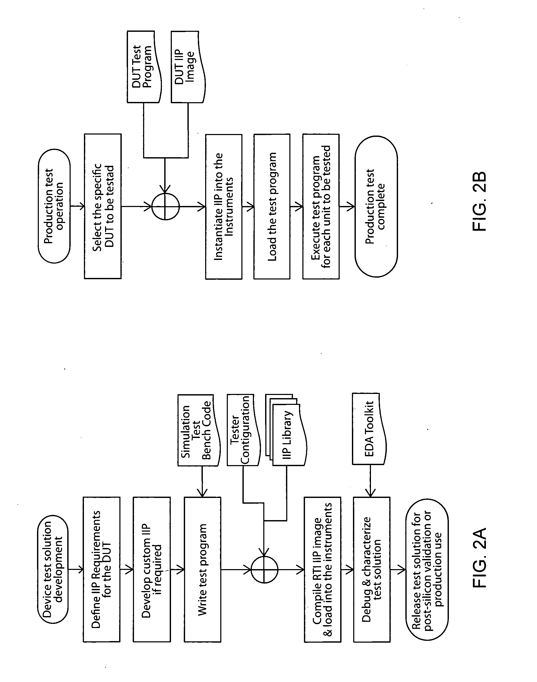
[0074]FIG. 9B shows the invention, where the TIP-based ATE instrument architecture replaces all four layers of the simulation testbench shown in FIG. 8. In this embodiment of the invention there is no connection to the simulator. The TIP has native random stimulus generation and response checking, As with the embodiment in FIG. 9A, the same EDA toolkit is available for debugging. This embodiment of the invention shows how the tools and methodology from pre-silicon verification are used for post-silicon validation, whereby similar test code can be used for stimulus and response checking of the DUT. Also, it's important to note that there are other embodiments of the invention that allow mixing of TIP test modes, random stimulus generation and response checking, and pre-defined stimulus and response checking, in the same TIP instance and across TIP instances. The invention is not limited to only this one embodiment.

third embodiment

[0075]FIG. 10A shows the invention, where the TIP-based ATE instrument architecture replaces the bottom three layers of the simulation testbench shown in FIG. 8. In this embodiment of the invention, the example simulation test program from FIG. 8 is used to pre-generate stimulus and response for all DUT interfaces, and write the data to one or more files in a predetermined format. The TIP-based ATE instrument architecture will then read the file or files, loading the specific stimulus and response into each TIP that connects to each DUT interface. This embodiment of the invention illustrates a “load and go” model that leverages the simulation testbench, but doesn't directly connect to it, which is applicable for production testing. Also note that the same EDA toolkit is available for debugging.

[0076]FIG. 10B shows a forth embodiment of the invention, where the TIP-based ATE instrument architecture replaces all four layers of the simulation testbench shown in FIG. 8. In this embodime...


PUM


Abstract

A test system based on multiple instances of reconfigurable instrument IP specifically matched to the device under test may be used in integrating automated testing of semiconductor devices between pre-silicon simulation, post-silicon validation, and production test phases, in one embodiment of software and hardware across all three phases, for different devices. The reconfigurable test system comprises: a tester instrument, instances of instrument IP instantiated in the tester instruments, a computer system, and a test program. The tester instrument connects to a device under test (DUT), and includes FPGAs reconfigurable for the three testing phases. The computer system has a user interface, and a controller connected to the reconfigurable tester instrument via a data bus. The test program stored on the controller, and the controller, instantiates interfaces and protocols, and certain process transactions to support the protocols, into FPGAs, to match device interfaces for each DUT, to execute test sequences.

Description

CROSS REFERENCES TO RELATED APPLICATIONS[0001]This application claims priority on U.S. Provisional Application Ser. No. 61 / 587,322 filed on Jan. 17, 2012, the disclosures of which are incorporated herein by reference.FIELD OF THE INVENTION[0002]The present invention relates to improvements in the architecture governing automatic test equipment, and more particularly to providing increased versatility and capability over fixed architecture instruments used in the testing of semiconductors.BACKGROUND OF THE INVENTION[0003]Semiconductor devices manufactured as integrated circuits may consist of billions of devices, including transistors, diodes, passives, MEMs, and other structures being built in and over a substrate that is typically a silicon wafer, which may undergo multiple microfabrication process steps, including doping, ion implantation, etching, deposition of various materials, and photolithographic patterning. The pin count of very large scale integration (VLSI) circuits has g...

Claims


Application Information

Patent Timeline
IPC IPC(8): G01R31/3177
CPCG01R31/3177G01R31/31908G01R31/2834
Inventor CZAMARA, ALLEN J.PAULSEN, EDALPEROVICH, LEV
Owner CZAMARA ALLEN J
Why Eureka
Try Eureka