Fin field effect transistor and fabrication method

a technology of fabrication method, which is applied in the direction of semiconductor devices, basic electric elements, electrical appliances, etc., can solve the problems of affecting the performance of the fin fet device, the critical dimension of the device further reducing, and the conventional mos field effect transistor (fet) is not able to meet the requirements of device performance, so as to facilitate a tight joint, reduce the leakage current of the gate, and reduce the defect of the ga

Active Publication Date: 2013-09-05
SEMICON MFG INT (SHANGHAI) CORP
View PDF6 Cites 12 Cited by
  • Summary
  • Abstract
  • Description
  • Claims
  • Application Information

AI Technical Summary

Benefits of technology

[0008]As disclosed herein, when the annealing process is performed in the presence of hydrogen-containing gas, atoms inside the fin can be recombined and lattice defects can be relieved. Because the repairing gas contains the element for forming the fin, during the annealing process, atoms corresponding to the material of the fin can be formed to fill a recess at the surface of the fin. The surface of the fin becomes sufficiently smooth to facilitate a tight joint between the gate structure and the surface of the fin. The formed Fin FET can thus have low gate leakage current and stable device performance.

Problems solved by technology

However, when critical dimensions of devices further decrease, even if the gate-last technology is used, conventional MOS field effect transistors (FETs) are not able to meet the requirements on the device performance.
However, when process nodes shrink further, problems may occur and affect performance of the Fin FET device.

Method used


Image

  • Fin field effect transistor and fabrication method
  • Fin field effect transistor and fabrication method
  • Fin field effect transistor and fabrication method

Examples


Embodiment Construction

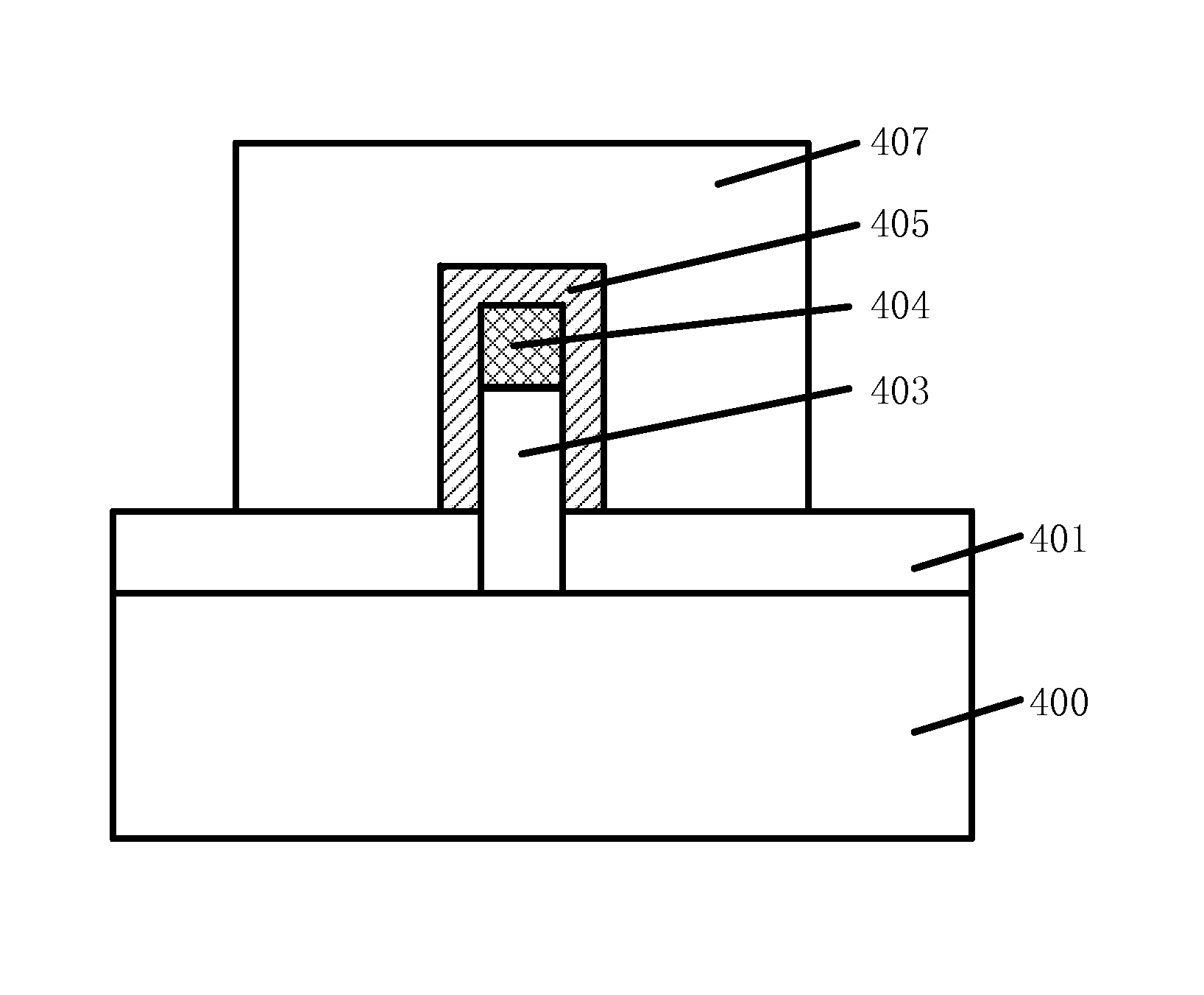
[0016]Reference will now be made in detail to exemplary embodiments of the disclosure, which are illustrated in the accompanying drawings. Wherever possible, the same reference numbers will be used throughout the drawings to refer to the same or like parts. For illustration purposes, elements illustrated in the accompanying drawings are not drawn to scale, which are not intended to limit the scope of the present disclosure. In practical operations, each element in the drawings has specific dimensions such as a length, a width, and a depth.

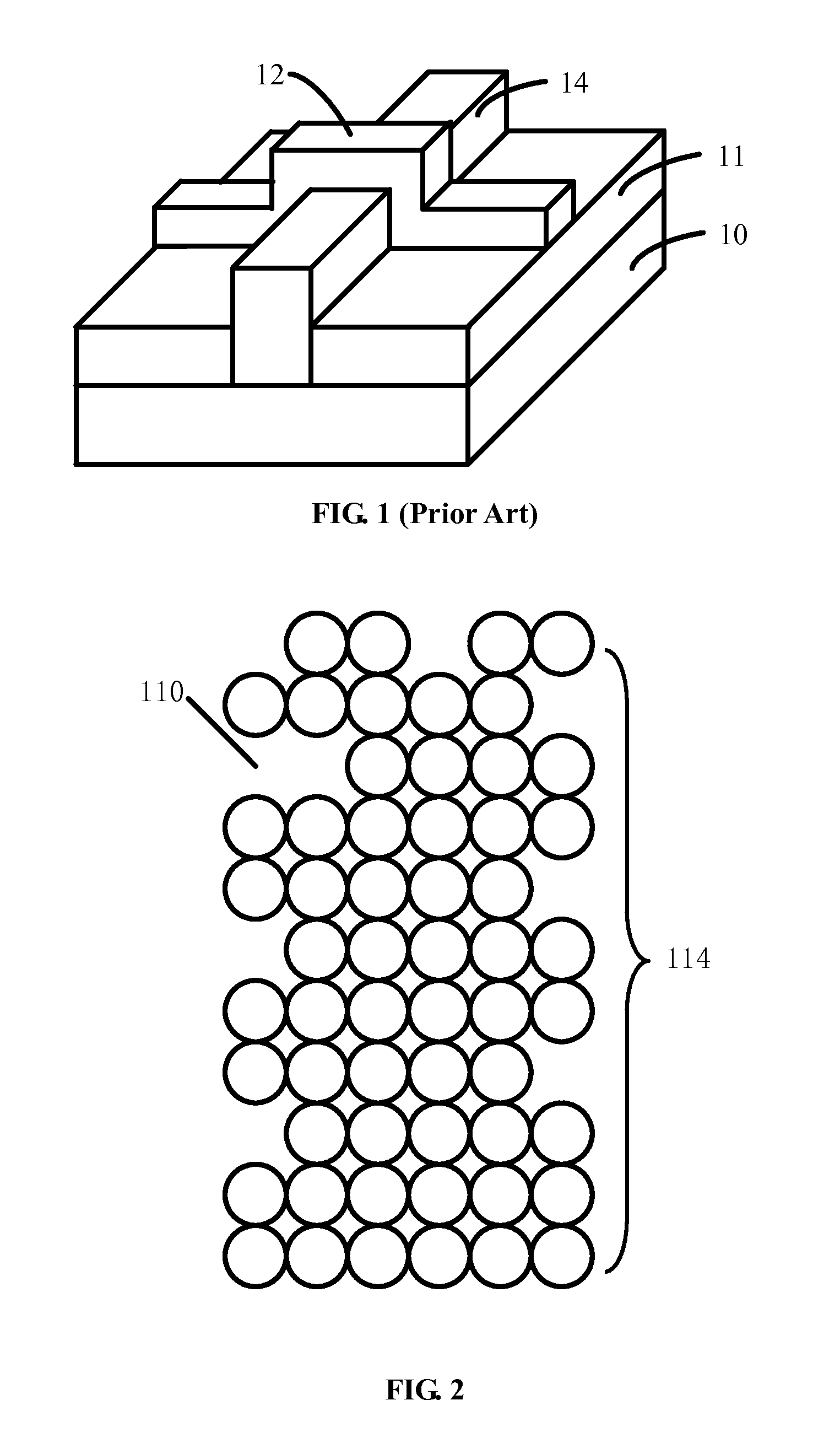
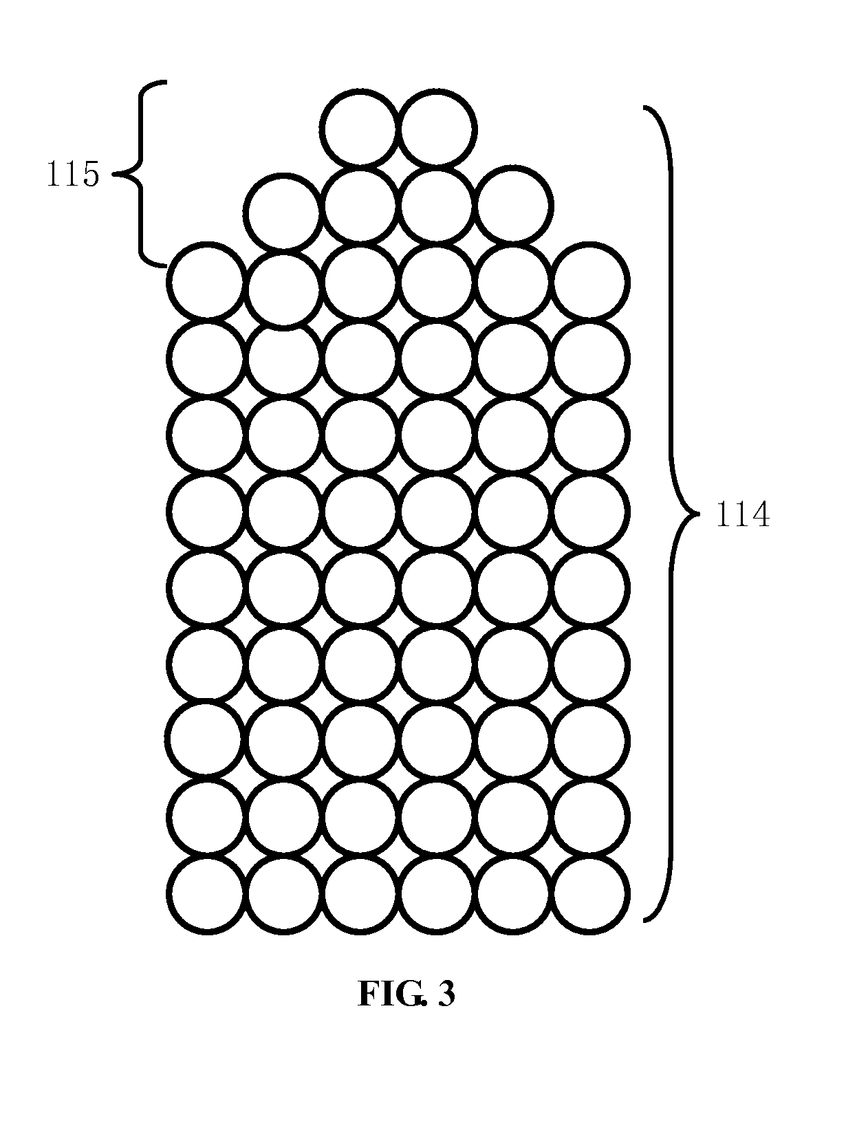
[0017]FIG. 2 is a microscopic schematic view illustrating a process for forming a fin field effect transistor. As shown in FIG. 2, when forming a fin 114, an etching process is often conducted using an etching gas. The etching gas may react with surface of the fin 114. A recess 110 may be formed on the surface of the fin 114, which may adversely affect formation and function of a subsequently-formed gate structure. For example, the gate structure a...


PUM


Abstract

A fin field effect transistor and a method for forming the fin field effect transistor are provided. In an exemplary method, the Fin FET can be formed by forming a dielectric layer and a fin on a semiconductor substrate. The fin can be formed throughout an entire thickness of the dielectric layer and a top surface of the fin is higher than a top surface of the dielectric layer. The fin can be annealed using a hydrogen-containing gas and a repairing gas containing at least an element corresponding to a material of the fin. A gate structure can be formed on the top surface of the dielectric layer and at least on sidewalls of a length portion of the fin after the annealing process.

Description

CROSS REFERENCE TO RELATED APPLICATIONS[0001]This application claims priority to Chinese patent application No. 201210054232.6, filed on Mar. 2, 2012 and entitled “METHOD FOR FORMING FIN FIELD EFFECT TRANSISTOR”, the entire disclosure of which is incorporated herein by reference.FIELD OF THE DISCLOSURE[0002]The present disclosure generally relates to the field of semiconductor manufacturing technology and, more particularly, to a fin field effect transistor (Fin FET) and a method for forming the Fin FET.BACKGROUND OF THE DISCLOSURE[0003]With increasing development of semiconductor technology, and with downsizing of process nodes, the gate-last technology has been widely used to achieve desired threshold voltage and to improve device performance. However, when critical dimensions of devices further decrease, even if the gate-last technology is used, conventional MOS field effect transistors (FETs) are not able to meet the requirements on the device performance. Thus, multi-gate devic...

Claims


Application Information

Patent Timeline
Patent Type & Authority Applications(United States)
IPC IPC(8): H01L29/66H01L29/78
CPCH01L29/7851H01L21/3247H01L29/785H01L29/66795
Inventor MIENO, FUMITAKE
Owner SEMICON MFG INT (SHANGHAI) CORP
Why Eureka
Try Eureka