Semiconductor device having penetrating electrodes each penetrating through substrate

Active Publication Date: 2013-09-05
LONGITUDE LICENSING LTD
View PDF6 Cites 46 Cited by
  • Summary
  • Abstract
  • Description
  • Claims
  • Application Information

AI Technical Summary

Benefits of technology

[0011]According to the present embodiment, bonding strength between stacked semiconductor chips can

Problems solved by technology

Therefore, it is difficult to stack many memory chips.
However, when the semiconductor chips are stacked, even as accurate positioning is carried out, the bonding strength between the semiconductor chips could be uneven i

Method used


Image

  • Semiconductor device having penetrating electrodes each penetrating through substrate
  • Semiconductor device having penetrating electrodes each penetrating through substrate
  • Semiconductor device having penetrating electrodes each penetrating through substrate

Examples


second embodiment

[0078]The following describes the present invention.

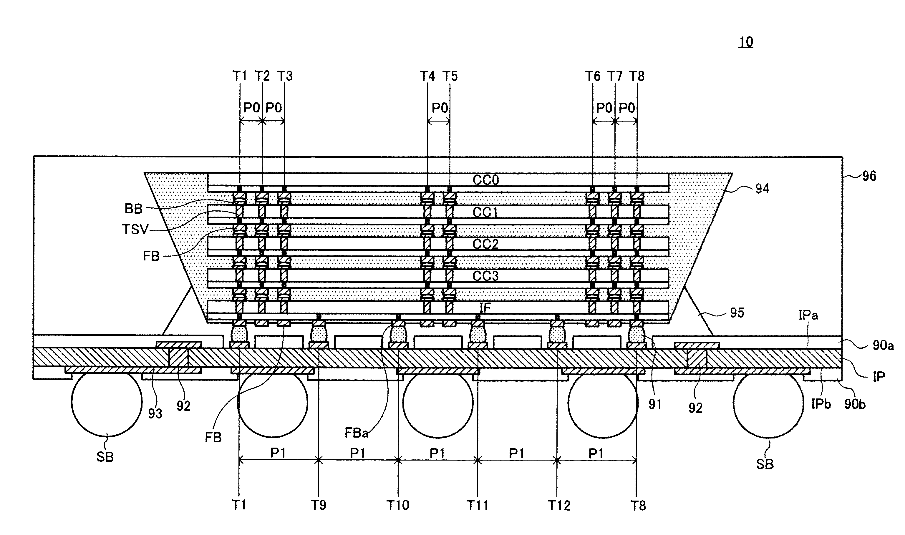
[0079]The positional accuracy of the substrate electrodes 91 on the interposer IP is lower than the positional accuracy of the penetrating electrodes TSV. Therefore, displacement of the substrate electrodes 91 can occur relative to the penetrating electrodes TSV. FIG. 11 shows the situation where the distance between a substrate electrode 91v1, which should be bonded to the penetrating electrode TSVv1, and a substrate electrode 91v2, which should be bonded to the penetrating electrode TSVv2, is shorter than a design value. If the substrate electrodes 91 remain displaced as described above during the process of stacking the chips, as shown in FIG. 11, there is a risk that the two substrate electrodes 91v1 and 91v2 come in contact with the same dummy penetrating electrode TSVd. The power supply potential VDD is supplied to the penetrating electrode TSVv1, and the power supply potential VSS to the penetrating electrode TSVv2. Therefor...

third embodiment

[0081]The following describes the present invention.

[0082]Turning to FIG. 13, according to the third embodiment, the dummy penetrating electrode TSVd at coordinate X0 between the power supply-assistance penetrating electrodes TSVv1a and TSVv2a, as well as the dummy penetrating electrode TSVd at coordinate X5 between the power-supply penetrating electrodes TVv1 and TSVv2, is removed. The configuration of the other components is the same as the layout shown in FIG. 8. As shown in FIGS. 14 and 15, which are cross-sectional views, even on the core chips CC1 to CC3, the penetrating electrodes TSV at coordinates X5 and X0 are removed. According to the present invention, the top-surface bump FB1 to back-surface bump BB8 shown in FIG. 14 may be referred to as “first bump” to “eighth bump”, respectively.

[0083]As described above with reference to FIG. 11, the power supply is short-circuited basically when the distance between the substrate electrodes 91v1 and 91v2 is narrower than the diamete...

fourth embodiment

[0084]The following describes the present invention.

[0085]Turning to FIG. 16, according to the present embodiment, the distance between the power-supply penetrating electrodes TSVv1 and TSVv2 is designed in advance so as to be wider than pitch P1. More specifically, while the distance between the power-supply penetrating electrodes TSVv1 and TSVv2 is pitch P1 according to the first to third embodiments, the distance is increased to P1+P0 according to the present embodiment. Therefore, between the power-supply penetrating electrodes TSVv1 and TSVv2, two dummy penetrating electrodes TSVd can be placed. Therefore, even if the substrate electrodes 91 are displaced or deformed, the power supply is not short-circuited. Moreover, there is no need to remove some of the dummy penetrating electrodes TSVd. Therefore, the formation density of the penetrating electrodes TSV can be increased to the same level as in the first embodiment.

[0086]It is apparent that the present invention is not limite...


PUM


Abstract

Disclosed herein is a device that includes: a first semiconductor chip having a first internal circuit formed in a first substrate; and a plurality of penetrating electrodes each penetrating through the first semiconductor substrate. The plurality of penetrating electrodes includes first, second, third and fourth penetrating electrodes arranged along a first line. The first and second penetrating electrodes are in a floating state without electrically connected to the first internal circuit. The third penetrating electrode is electrically connected to a first power supply line that conveys a first power supply potential to the first internal circuit. The fourth penetrating electrode is electrically connected to a second power supply line that conveys a second power supply potential to the first internal circuit. The third and fourth penetrating electrodes are arranged between the first penetrating electrode and the second penetrating electrode.

Description

BACKGROUND OF THE INVENTION[0001]1. Field of the Invention[0002]The present invention relates to a semiconductor device, and particularly to a semiconductor device equipped with a penetrating electrode which is so provided as to pass through a substrate.[0003]2. Description of Related Art[0004]Storage capacity required for semiconductor memory devices such as DRAM (Dynamic Random Access Memory) has been growing year by year. To satisfy the requirement, in recent years, a memory device called multi-chip package has been proposed. In the multi-chip package, a plurality of memory chips are stacked. However, in the case of the multi-chip package, a wire needs to be provided for each chip to connect each memory chip and a package substrate. Therefore, it is difficult to stack many memory chips.[0005]On the other hand, in recent years, a semiconductor device of a type in which a plurality of memory chips with penetrating electrodes are stacked has been proposed (See Japanese Patent Applic...

Claims


Application Information

Patent Timeline
IPC IPC(8): H01L23/48
CPCH01L23/481H01L23/3128H01L23/49816H01L21/563H01L2224/16145H01L2224/16225H01L2924/15311H01L23/562H01L23/585H01L25/0657H01L25/18H01L2225/06517H01L2225/06513H01L2225/06544H01L23/3135
Inventor IDE, AKIRA
Owner LONGITUDE LICENSING LTD
Why Eureka
Try Eureka