
Surface-emitting laser array, optical scanning device, and image forming device

a laser array and surface-emitting technology, applied in the direction of lasers, laser optical resonator construction, laser details, etc., can solve the problems of difficult to carry out uniform mesa etching on the surface of the wafer, difficult to control the depth of etching, and difficult to carry out mesa etching. the effect of preventing the exposure preventing the oxidization of the first reflection layer

Active Publication Date: 2013-09-05
RICOH KK
View PDF2 Cites 4 Cited by
  • Summary
  • Abstract
  • Description
  • Claims
  • Application Information

AI Technical Summary

Benefits of technology

This design effectively prevents heat accumulation in the active layer, enhancing the optical output and extending the lifespan of the surface-emitting laser array while maintaining high-density array arrangements without the complications of dummy elements.

Problems solved by technology

However, from the problem of the controllability of the etching depth, it is difficult to control the etching bottom to be deeper than the selective oxidation layer but not to reach the lower semiconductor Bragg reflector.
Practically, it is very difficult to carry out mesa etching so as be deeper than the selective oxidation layer but not to reach the lower semiconductor Bragg reflector.
However, in the case of the surface-emitting laser array, carrying out uniform mesa etching within the surface of the wafer is still more difficult for other additional reasons.
If the oxidation rate of the low refractive index layer of the lower semiconductor Bragg reflector is quicker than the selective oxidation layer, the whole low refractive index layer is oxidized early and performing the current pouring is impossible.
There are the problems that the optical output declines and the life of the surface-emitting laser element becomes short.
Especially, when the surface-emitting laser array operates, undesired influences due to thermal interference become remarkable.
Operation of the surface-emitting laser array at high current values is impossible and use of the surface-emitting laser array with a low optical output is unavoidable.
And the life of the surface-emitting laser array becomes short due to a temperature rise caused by thermal interference.
This causes monitoring of oxidization (plasma emission spectrometry, optical reflective index analysis, etc.) to be difficult to perform.
Moreover, if the dummy elements are arranged in the whole wafer, unevenness appears on the surface of the laser array and the probability of wire cut-off is raised.
However, if unevenness exists under the bottom of the bonding pads, the mesa structure may be damaged at the time of wire bonding, which causes a faulty surface-emitting laser array to be produced.

Method used


Image

  • Surface-emitting laser array, optical scanning device, and image forming device
  • Surface-emitting laser array, optical scanning device, and image forming device
  • Surface-emitting laser array, optical scanning device, and image forming device

Examples


Embodiment Construction

[0087]A description will be given of embodiments of the invention with reference to the accompanying drawings.

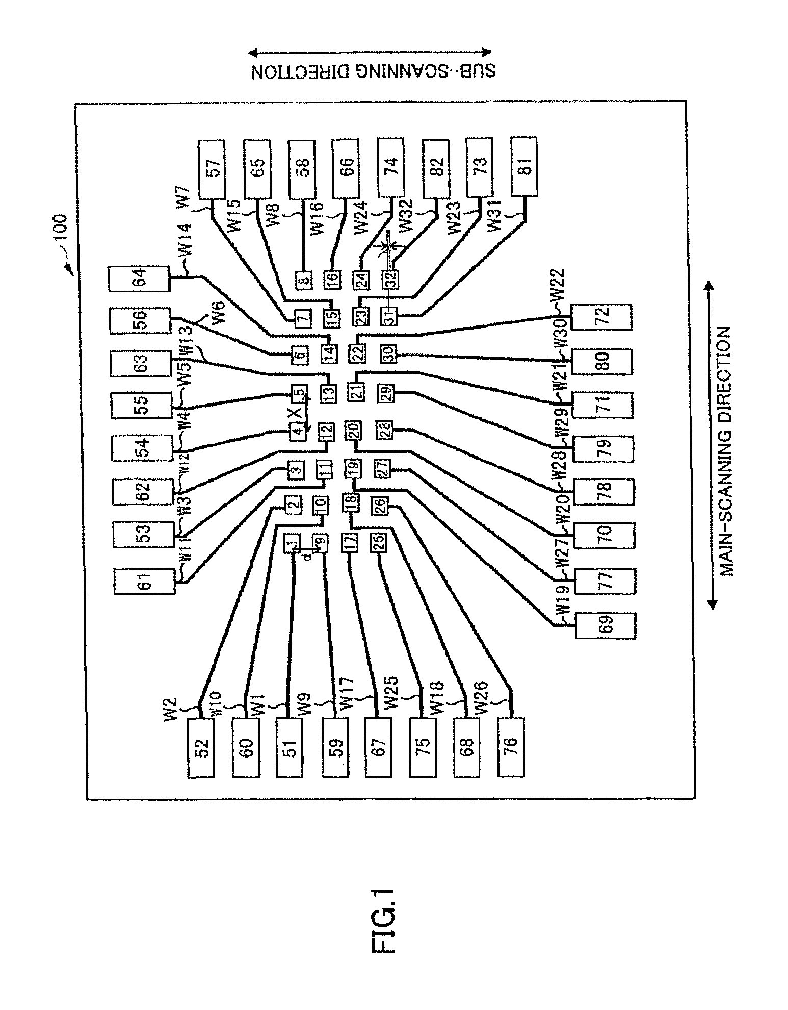
[0088]FIG. 1 is a plan view of a surface-emitting laser array in an embodiment of the invention. As shown in FIG. 1, the surface-emitting laser array 100 of this embodiment includes surface-emitting laser elements 1-32, pads 51-82, and wires W1-W32.

[0089]The surface-emitting laser elements 1-32 are arranged in the two-dimensional formation of four rows×eight columns. Each of the surface-emitting laser elements 1-32 has the rectangle form whose one side is 16 micrometers.

[0090]And the columns of four surface-emitting laser elements 1,9,17,25 / 2,10,18,26 / 3,11,19,27 / 4,12,20,28 / 5,13,21,29 / 6,14,22,30 / 7,15,23,31 / 8,16,24,32 are arranged in the sub-scanning direction. And the rows of eight surface-emitting laser elements 1-8 / 9-16 / 17-24 / 25-32 are arranged in the main scanning direction.

[0091]The rows of the eight surface-emitting laser elements 1-8 / 9-16 / 17-24 / 25-32 arranged in the mai...


PUM


Abstract

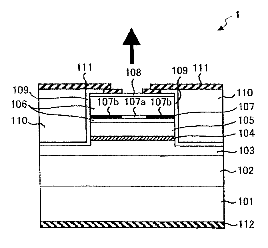
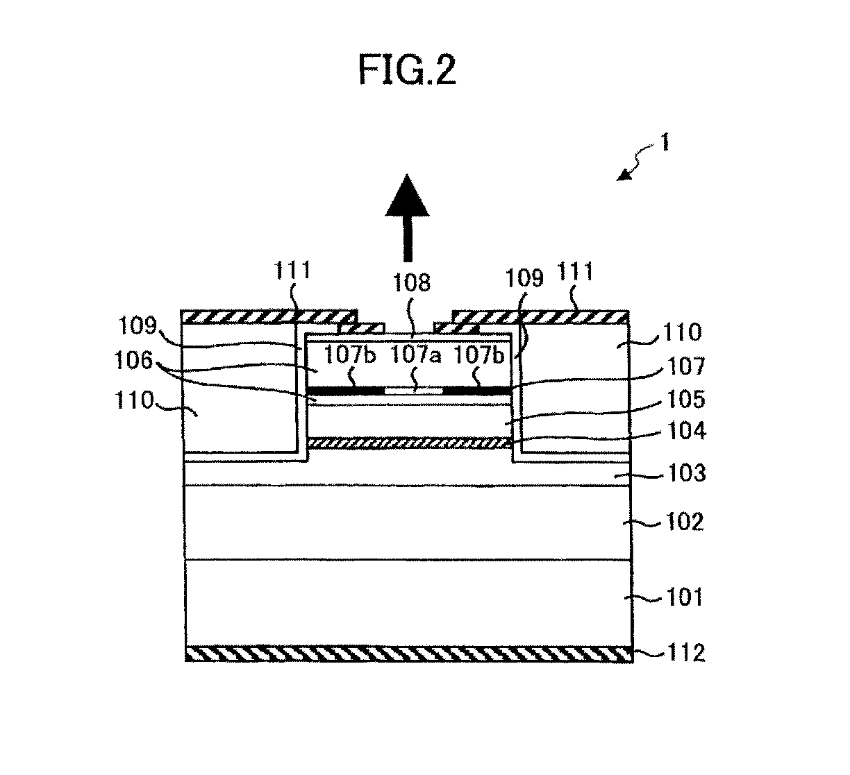
A surface-emitting laser array includes a plurality of surface-emitting laser elements. Each surface-emitting laser element includes a first reflection layer formed on a substrate, a resonator formed in contact with the first reflection layer and containing an active layer, and a second reflection layer formed over the first reflection layer and in contact with the resonator. The second reflection layer contains a selective oxidation layer. The first reflection layer contains on the active layer side at least a low refractive index layer having an oxidation rate equivalent to or larger than an oxidation rate of a selective oxidation layer contained in the second reflection layer. The resonator is made of an AlGaInPAs base material containing at least In. A bottom of a mesa structure is located under the selective oxidation layer and over the first reflection layer.

Description

TECHNICAL FIELD[0001]This invention relates to a surface-emitting laser array, an optical scanning device including the surface-emitting laser array, and an image forming device including the surface-emitting laser array.BACKGROUND ART[0002]In a surface-emitting laser array in which surface-emitting laser elements are integrated, the output of each surface-emitting laser element during operation may decline due to a temperature rise through reception of heat from the surrounding surface-emitting laser elements, and the life of the surface-emitting laser array may be shortened.[0003]To obviate the problem, it is necessary to improve the heat dissipation characteristic. For example, a material having a high thermal conductivity should be used for a semiconductor Bragg reflector which is located on the side of main heat dissipation. Among the materials which can be used for a semiconductor Bragg reflector of a surface-emitting laser element on a GaAs substrate, AlAs is a suitable one t...

Claims


Application Information

Patent Timeline
Patent Type & Authority Applications(United States)
IPC IPC(8): H01S5/18H01S5/185
CPCB82Y20/00H01S5/0203H01S5/18313H01S5/18358H01S5/18H01S5/3434H01S5/423H01S2302/00H01S5/2213H01S5/185H01S5/183H01S5/42
Inventor SATO, SHUNICHIITOH, AKIHIROSUGAWARA, SATORUSHOUJI, HIROYOSHI
Owner RICOH KK
Learn More