Detection apparatus, exposure apparatus, and method of manufacturing device
a technology of detection apparatus and manufacturing device, which is applied in the direction of optical radiation measurement, instruments, spectrometry/spectrophotometry/monochromators, etc., can solve the problems of lowering throughput, measurement operation taking a considerable time, and it is difficult to observe the alignment mark positioned at an arbitrary position on the lower surface of the wafer, etc., to achieve accurate detection of the position of the mark formed
- Summary
- Abstract
- Description
- Claims
- Application Information
AI Technical Summary
Benefits of technology
Problems solved by technology
Method used
Image
Examples
first embodiment
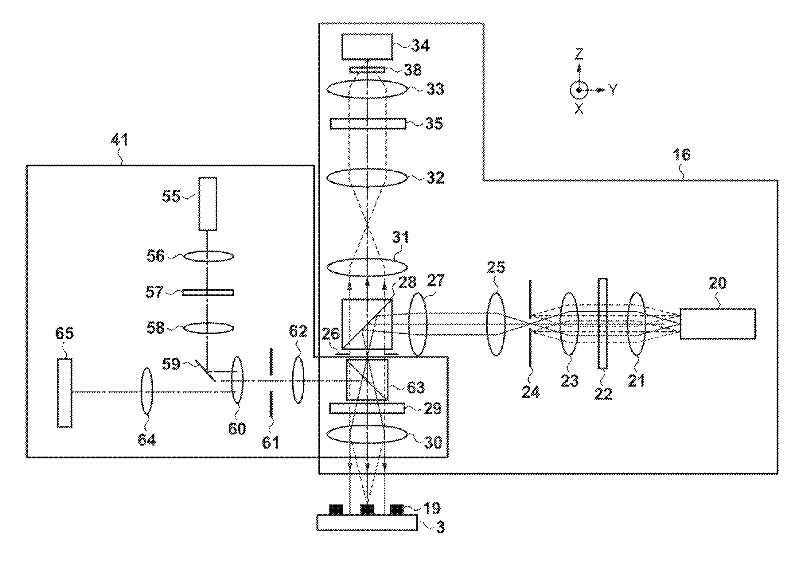
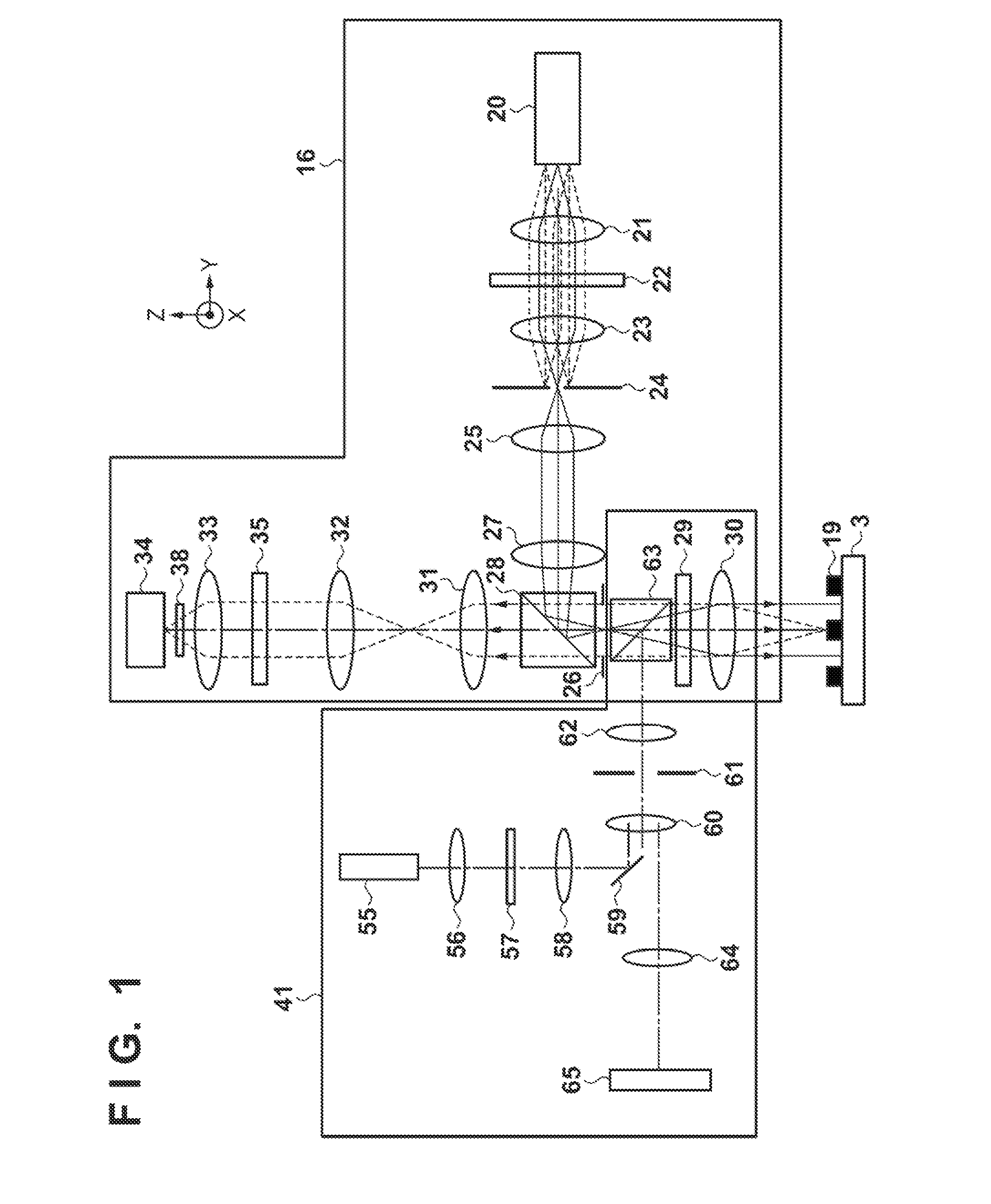
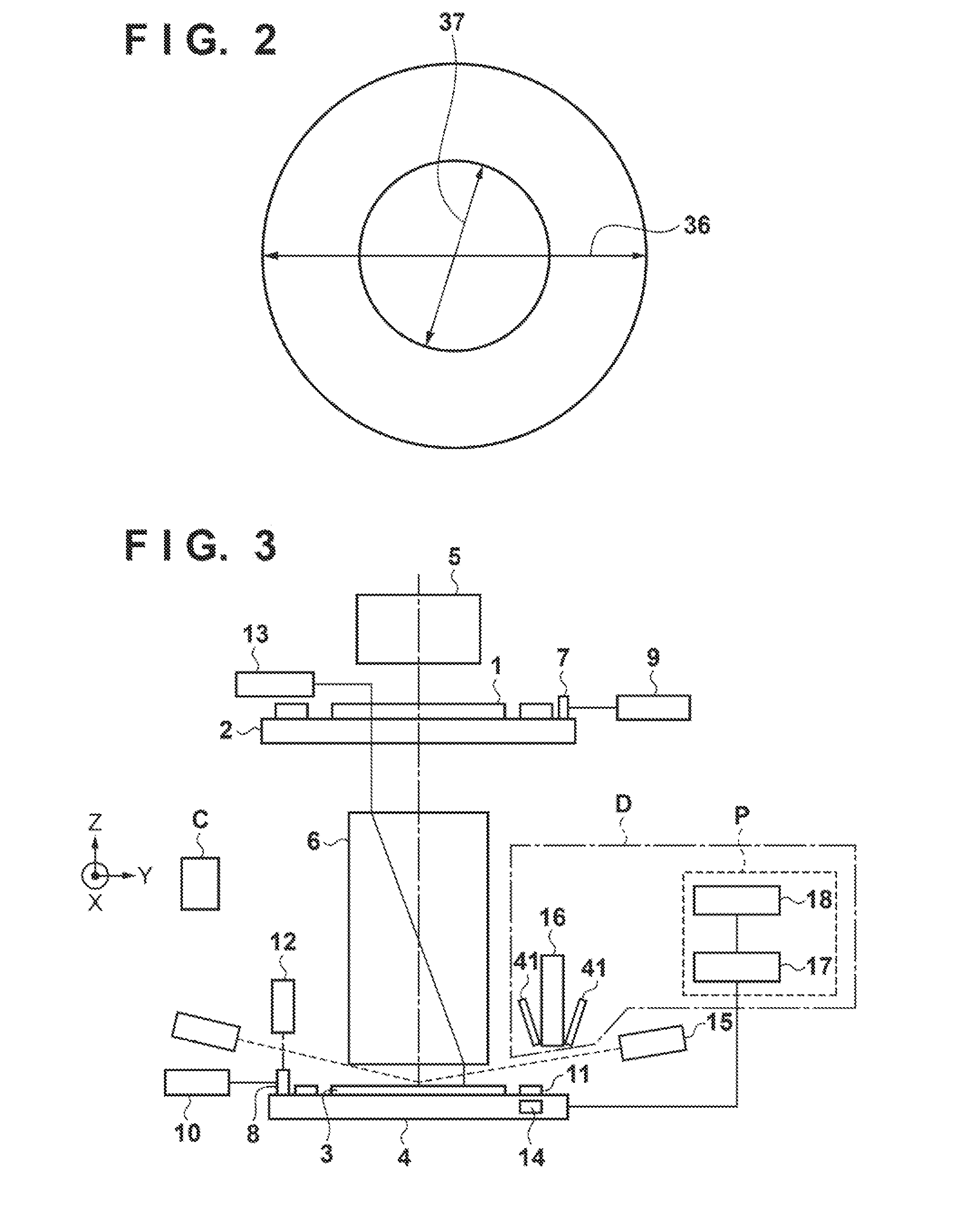
[0037]An exposure apparatus capable of measuring an alignment mark (mark) 19 on the lower surface of a wafer (target object) 3 at high speed and high accuracy, based on the thickness and refractive index of the target object, will be described with reference to FIG. 3. The exposure apparatus includes a detection apparatus including a wafer alignment detector (first detector) 16 shown in FIG. 1, and a focus detector (second detector) 41 which assists in detecting a best focus position of the wafer alignment detector 16 by detecting the upper surface position of the wafer 3. The focus detector (second detector) 41 will be referred to as an “AF detector” hereinafter. The exposure apparatus also includes a reticle stage 2, wafer stage (substrate stage) 4, illumination optical system 5, projection optical system 6, and control unit C. The reticle stage 2 supports a reticle (mask) 1. The wafer stage 4 supports the wafer (substrate) 3. The illumination optical system 5 illuminates the reti...
second embodiment
[0071]In the first embodiment, the focus position of the wafer alignment detector 16 relative to the mark 19 formed on the lower surface of the wafer 3 is quickly obtained using the focus detectors 41 and 67 which detect the upper surface position of the wafer 3. In the second embodiment, a wafer alignment detector which can switch between two detection modes: first and second detection modes is used as a wafer alignment detector 16. Also, in the second embodiment, the focus detectors 41 and 67 which detect the upper surface position of the wafer 3, that are used in the first embodiment, are not used. The wafer alignment detector 16 detects a mark 19 with a first detection accuracy while changing the interval between marks 19 at a first pitch in the first detection mode, and detects the mark 19 with a second detection accuracy while changing the interval between the marks 19 at a second pitch in the second detection mode. In this case, the second pitch is smaller than the first pitc...
PUM
 Abstract
Description
Claims
Application Information


