Eureka AIR delivers breakthrough ideas for toughest innovation challenges, trusted by R&D personnel around the world.

Method for fabricating semiconductor device

Active Publication Date: 2013-09-05
UNITED MICROELECTRONICS CORP
View PDF6 Cites 0 Cited by
  • Summary
  • Abstract
  • Description
  • Claims
  • Application Information

AI Technical Summary

Benefits of technology

The patent text proposes a solution to the problem of voids and gaps that can occur during the process of forming a tensile stress-inducing dielectric layer. By removing the capping layers prior to the subsequent process, such as the process for forming an interconnection, the drawbacks and problems caused by the voids and gaps can be avoided. This results in a higher yield of semiconductor devices and prevents the problems caused by metal leads extending along the voids and gaps.

Problems solved by technology

However, the semiconductor device still suffers some problems as each technology nodes shrink and the dimension and element pitch of the semiconductor device are reduced.
For example, during the UV curing step, voids or gaps may occur in these aforementioned material layers due to the stress gain and the difference of expansion rate between the different material layers.
As a result, some undesired metal leads may occur on the metal lines or plugs generated by a subsequent interconnection process and extend along those voids.
At the worst, the semiconductor device may be shortened out by those metal leads.

Method used


Image

  • Method for fabricating semiconductor device
  • Method for fabricating semiconductor device
  • Method for fabricating semiconductor device

Examples


Embodiment Construction

[0022]A method for fabricating a semiconductor device is provided to form a DSL on a CMOS transistor element of the semiconductor device in order to improve the performance and the yield of the semiconductor device. The present invention will now be described more specifically with reference to the following embodiments. It is to be noted that the following descriptions of preferred embodiments of this invention are presented herein for purpose of illustration and description only. It is not intended to be exhaustive or to be limited to the precise form disclosed.

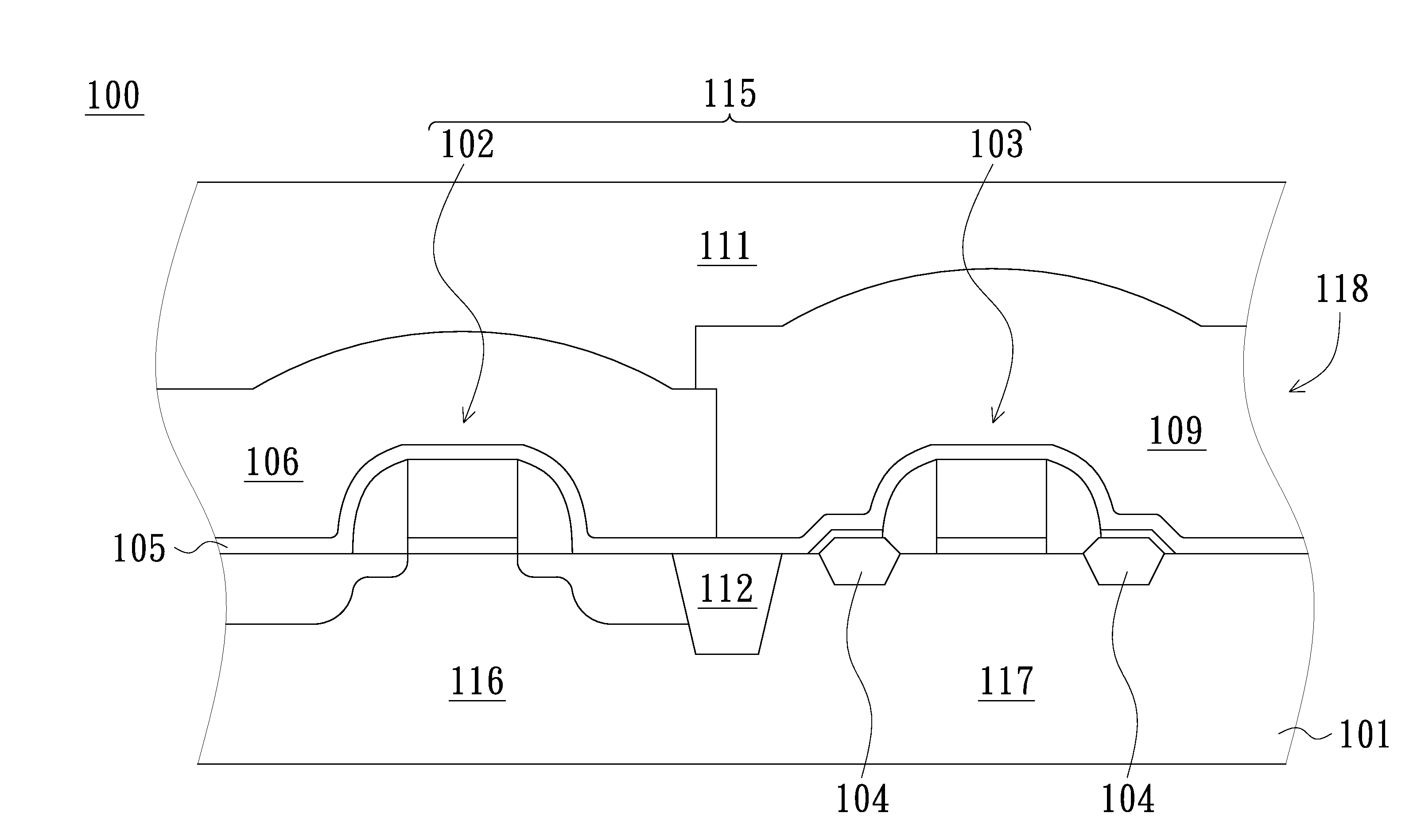
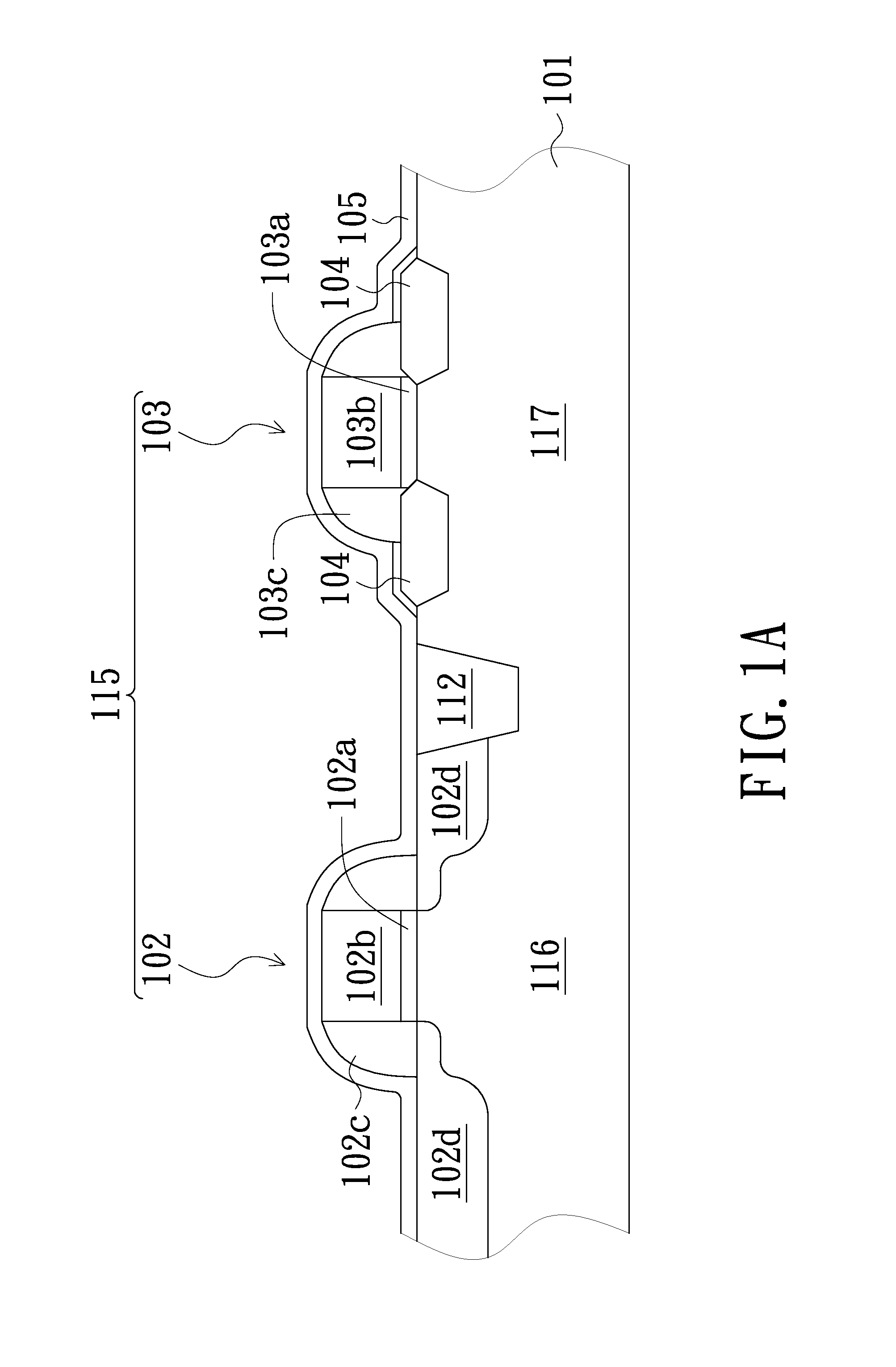
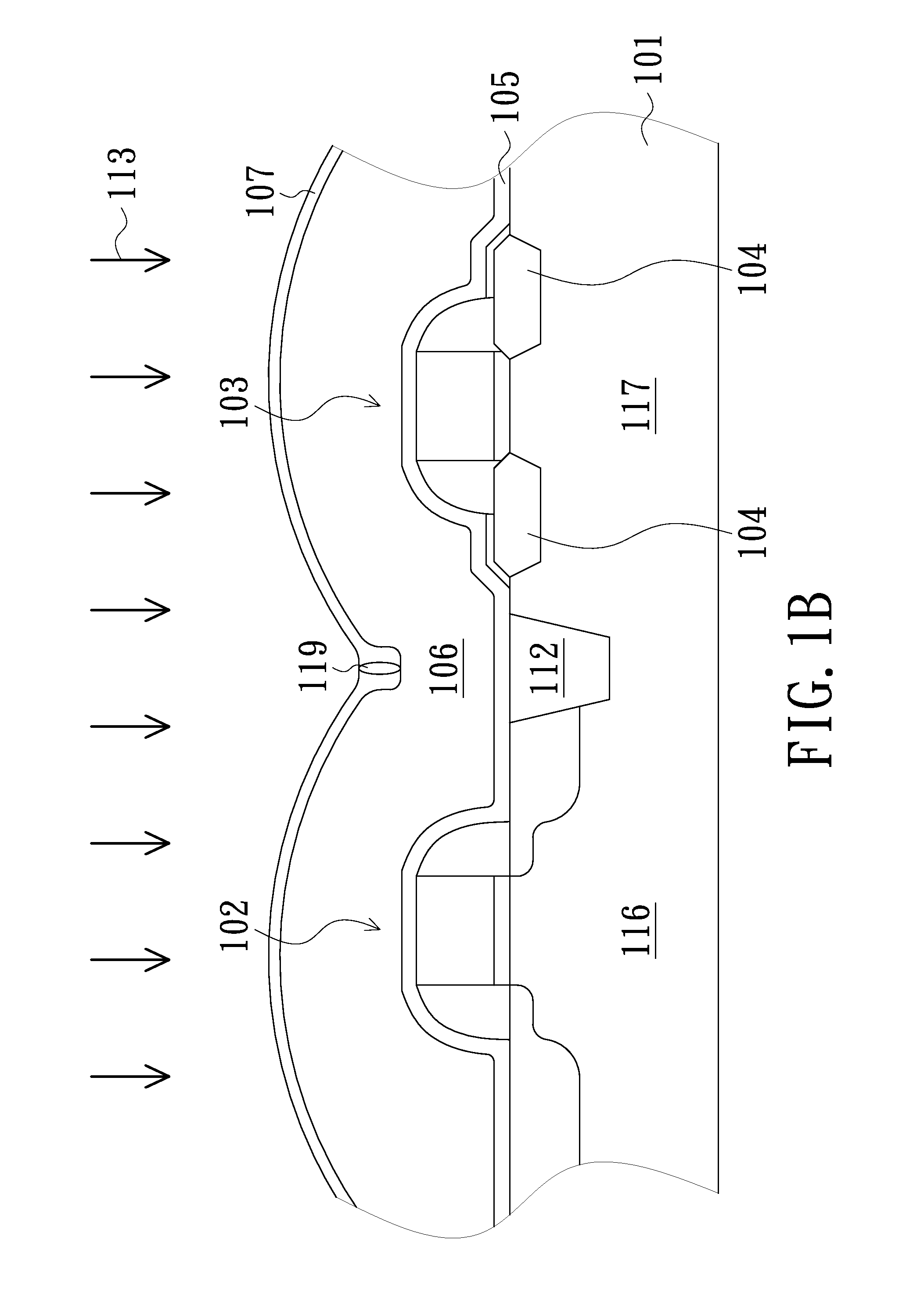
[0023]FIGS. 1A through 1G illustrate cross-sectional views of a method for fabricating a semiconductor device 100 in accordance with one embodiment of the present invention, wherein the semiconductor device 100 has at least one CMOS transistor element 115 and a DSL 118 form on the CMOS transistor element 115.

[0024]The method for fabricating the semiconductor device 100 comprises steps as follows: A CMOS transistor element 1...


PUM


Abstract

A method for fabricating a semiconductor device is provided, wherein the method comprises steps as follows: A first conductive-type metal-oxide-semiconductor transistor and a second conductive-type metal-oxide-semiconductor transistor are firstly formed on a substrate. Subsequently, a first stress-inducing dielectric layer and a first capping layer are formed in sequence on the first conductive-type metal-oxide-semiconductor transistor; and then a second stress-inducing dielectric layer and a second capping layer are formed in sequence on the second conductive-type metal-oxide-semiconductor transistor. Next, the fist capping layer is removed.

Description

FIELD OF THE INVENTION[0001]The present invention relates to a method for fabricating a semiconductor device, and more particularly to a method for fabricating a semiconductor device with a stress-inducing dielectric layer.BACKGROUND OF THE INVENTION[0002]A metal-oxide-semiconductor field effect transistor (MOSFET) is currently one of the most promising elements applied by a semiconductor device, due to the superior characteristics in view of operating speed and / or power consumption and cost efficiency.[0003]Currently, in order to further enhance the performance of the MOSFET, a strained-Si channel technology, such as utilizing a contact etch stop layer (CESL) with compress / strain stress (referred as stress-inducing CESL), is applied to raise the channel carrier mobility of MOSFETs.[0004]To take a stress-inducing CESL as an example, its formation may comprises following steps: A silicon nitride (SiN) dielectric layer covering on a transistor are firstly provided, and an ultra-violat...

Claims


Application Information

Patent Timeline
IPC IPC(8): H01L21/8238
CPCH01L21/823807H01L29/7848H01L29/7843H01L21/823814
Inventor LIU, AN-CHITENG, CHIH-WENTSENG, TZU-YULIN, CHI-HENG
Owner UNITED MICROELECTRONICS CORP
Why Eureka
Eureka Blog
Learn More