Interposer substrate manufacturing method and interposer substrate

Inactive Publication Date: 2013-09-12
THE FUJIKURA CABLE WORKS LTD
View PDF10 Cites 19 Cited by
  • Summary
  • Abstract
  • Description
  • Claims
  • Application Information

AI Technical Summary

Benefits of technology

[0033]Therefore, according to the present invention, it is possible to provide an interposer substrate having improved electrical stability of the throug

Problems solved by technology

In particular, when a through hole is formed vertically and an insulating material is also formed similarly vertically for the hole shape, there is a problem in that defects, such as poor electrical conduction or wire breakage, are easily caused since a conductive material is thin in the vicinity of the bottom surface portion when forming a conductive layer on the seed layer.
For this reason, it is difficult to improve

Method used


Image

  • Interposer substrate manufacturing method and interposer substrate
  • Interposer substrate manufacturing method and interposer substrate
  • Interposer substrate manufacturing method and interposer substrate

Examples


Embodiment Construction

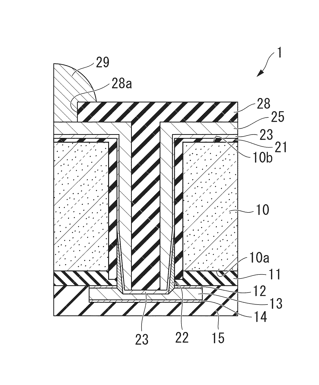
[0046]Hereinafter, an interposer substrate manufacturing method and an interposer substrate according to an embodiment of the present invention will be described referring to the drawings.

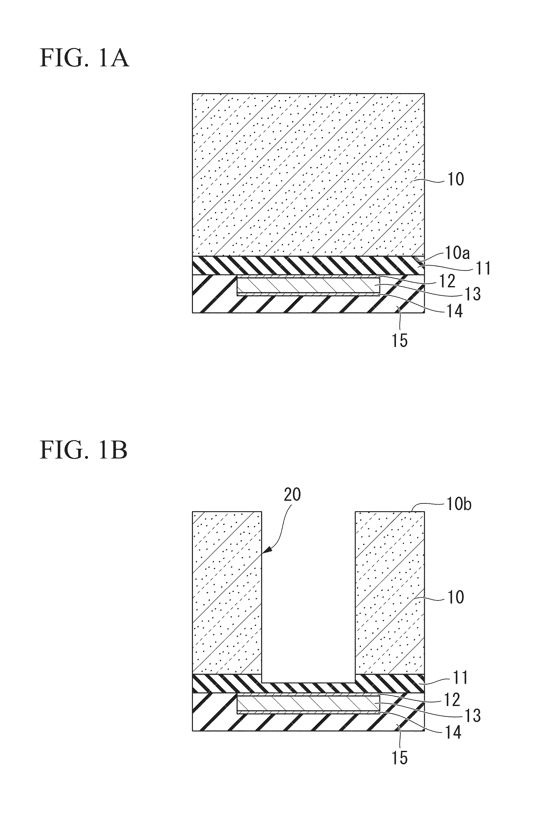
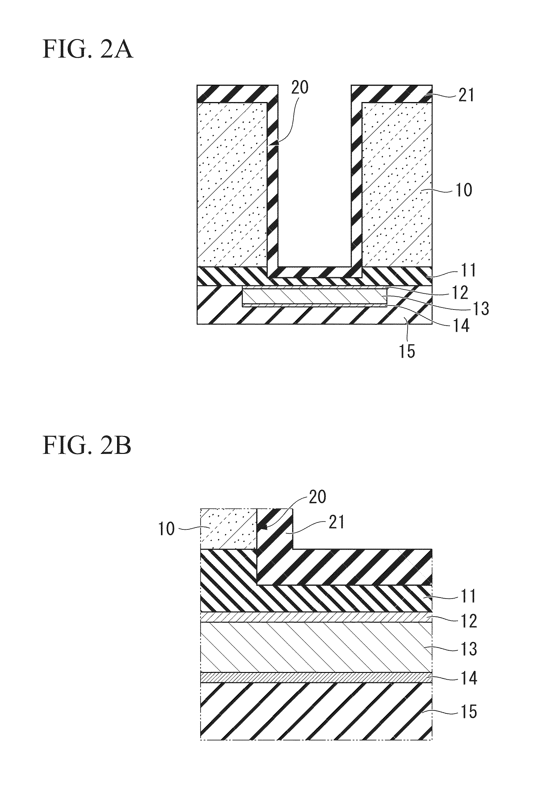
[0047]FIGS. 1A to 4B are cross-sectional views schematically showing the interposer substrate manufacturing method according to the present embodiment.

[0048]The interposer substrate manufacturing method according to the present embodiment is a method for manufacturing an interposer substrate 1 including: a first step of forming a conductive portion (for example, an electrode, a wiring, and the like) 13, which is formed of a first metal, on one surface (first surface) 10a of a semiconductor substrate 10 with a first insulating layer 11 interposed therebetween; a second step of forming a through hole 20 at a other surface (second surface) 10b side of the semiconductor substrate 10 located on an opposite side to the first surface so as to expose the first insulating layer 11; a third step of forming a...


PUM


Abstract

A method for manufacturing an interposer substrate includes: forming a conductive portion on a first surface of a semiconductor substrate via a first insulating layer, the conductive portion being formed of a first metal; forming a through hole at a second surface side of the semiconductor substrate located on an opposite side to the first surface so as to expose the first insulating layer; forming a second insulating layer on at least an inner wall surface and a bottom surface of the through hole; exposing the conductive portion by removing portions of the first and second insulating layers using a dry etching method that uses an etching gas containing a fluorine gas, the portions of the first and second insulating layers being located on the bottom surface of the through hole; and forming a conductive layer on the second insulating layer and electrically connecting the conductive layer to the conductive portion, wherein when exposing the conductive portion, forming a tapered portion is performed.

Description

CROSS REFERENCE TO RELATED APPLICATIONS[0001]This application is a continuation application based on a PCT Patent Application No. PCT / JP2011 / 074664, filed Oct. 26, 2011, whose priority is claimed on Japanese Patent Application No. 2010-243873, filed Oct. 29, 2010, the entire content of which are hereby incorporated by reference.BACKGROUND OF THE INVENTION[0002]1. Field of the Invention[0003]The present invention relates to an interposer substrate manufacturing method and an interposer substrate.[0004]2. Description of the Related Art[0005]In recent years, electronic apparatuses, such as mobile phones, have higher functionality, development to achieve miniaturization and higher performance of optical devices themselves including electronic devices, such as ICs or LSIs, and optical devices, such as OEICs or optical pickups, is being made in various places.[0006]For example, a technique for providing these devices by stacking has been proposed.[0007]Specifically, there is an interposer...

Claims


Application Information

Patent Timeline
IPC IPC(8): H01L21/768H01L23/48
CPCH01L21/76898H01L23/481H01L2924/1461H01L2224/0401H01L2224/131H01L21/76843H01L2224/05H01L2224/02372H01L2224/05548H01L2224/13022H01L2224/13024H01L2924/014H01L2924/00H01L23/49827H01L23/147H01L21/76805
Inventor ONAI, SATOSHI
Owner THE FUJIKURA CABLE WORKS LTD
Why Eureka
Try Eureka