

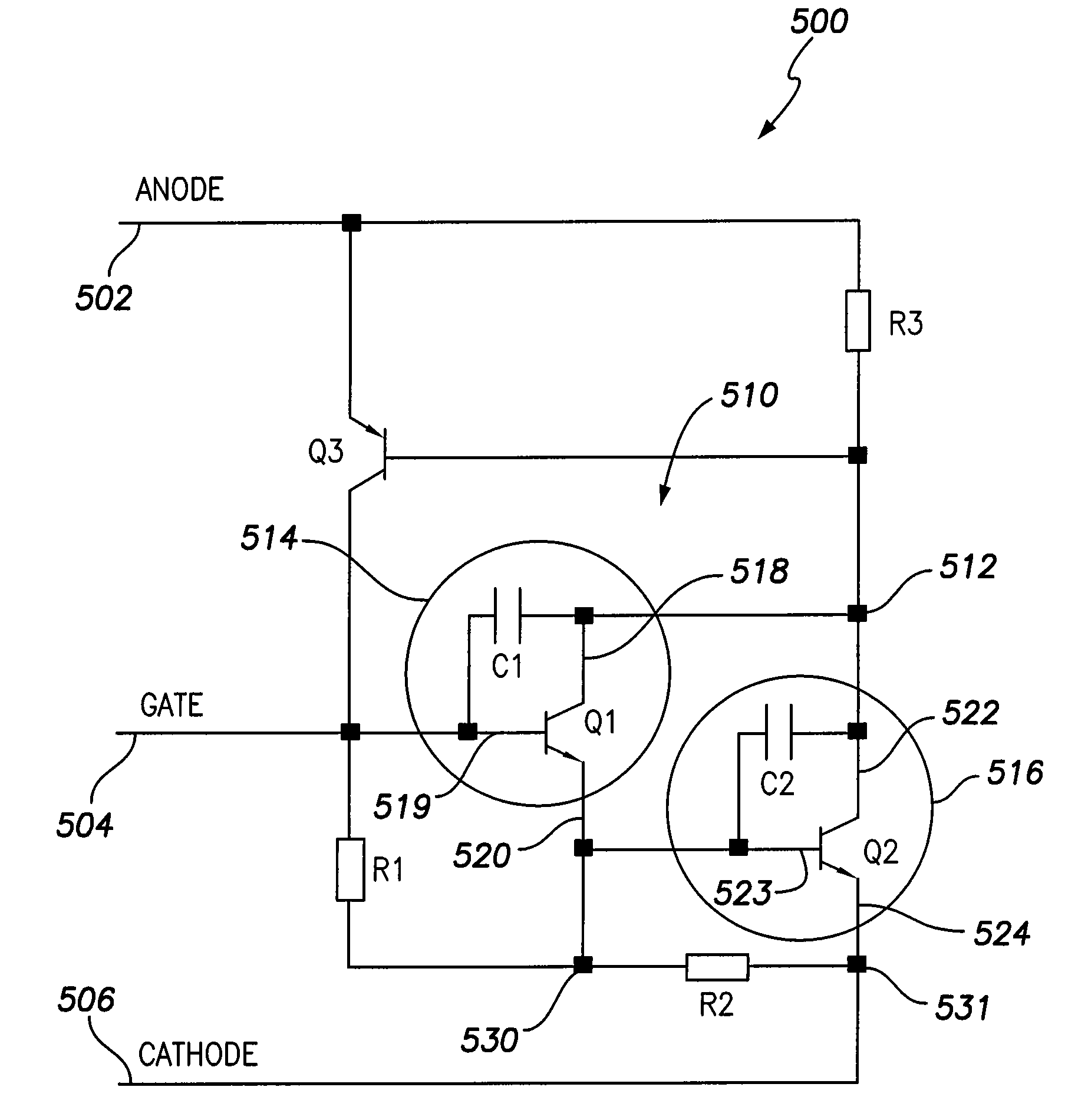
Methods and systems for implementing an SCR topology in a high voltage switching circuit
a high-voltage switching circuit and topology technology, applied in the field of medical devices, can solve the problems of increasing the die size of cmos, affecting the operation of the circuit,
- Summary
- Abstract
- Description
- Claims
- Application Information
AI Technical Summary
Benefits of technology
Problems solved by technology
Method used
Image

Examples
Embodiment Construction
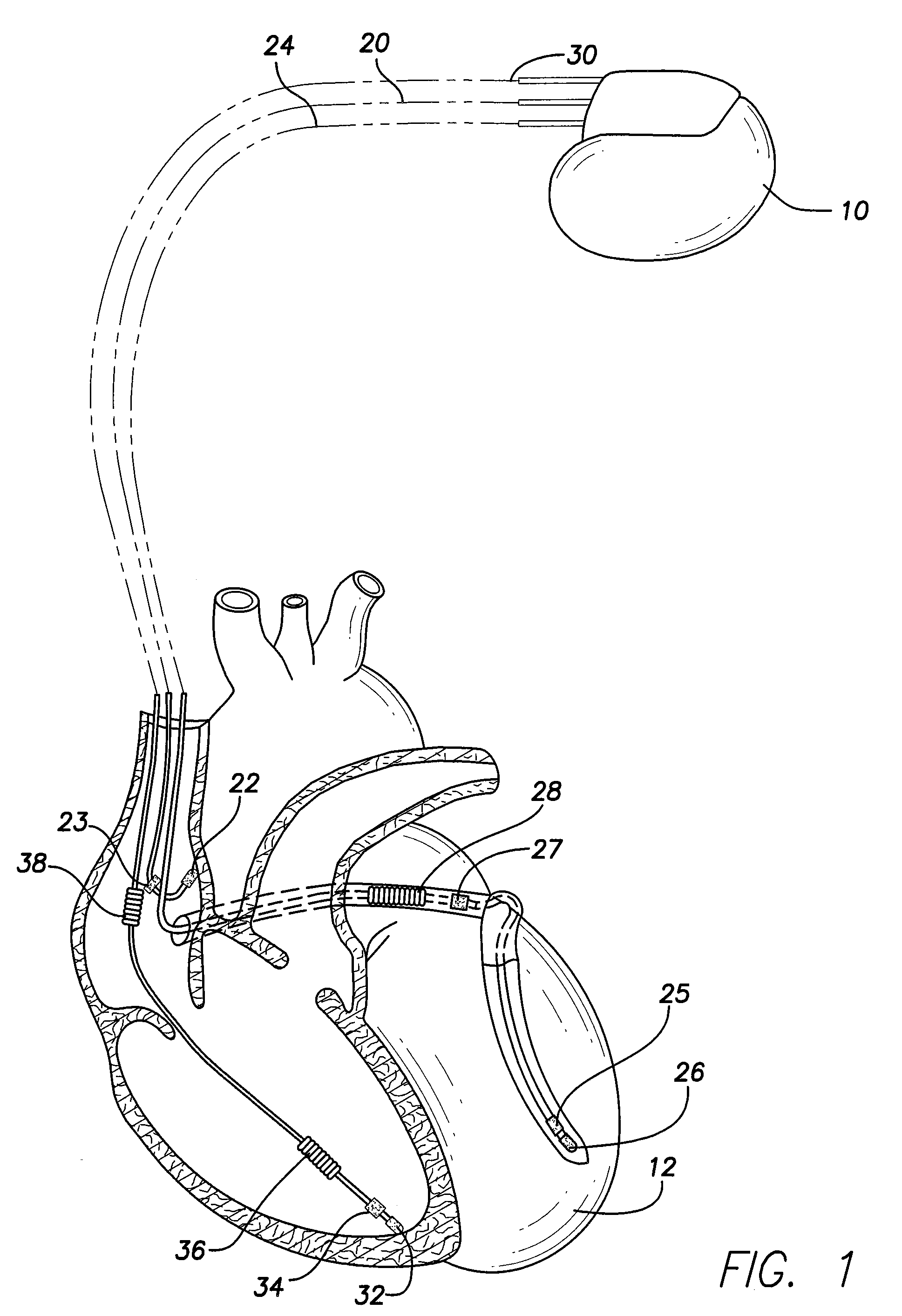
[0033]FIG. 1 illustrates an IMD 10 in electrical communication with a patient's heart 12 by way of three leads 20, 24 and 30 suitable for delivering multi-chamber stimulation and / or shock therapy. To sense atrial cardiac signals and to provide right atrial chamber stimulation therapy, the IMD 10 is coupled to an implantable right atrial lead 20 including at least one atrial tip electrode 22 that typically is implanted in the patient's right atrial appendage. The right atrial lead 20 may also include an atrial ring electrode 23 to allow bipolar stimulation or sensing in combination with the atrial tip electrode 22.
[0034]To sense the left atrial and left ventricular cardiac signals and to provide left-chamber stimulation therapy, the IMD 10 is coupled to a “coronary sinus” lead 24 designed for placement in the “coronary sinus region” via the coronary sinus ostium in order to place a distal electrode adjacent to the left ventricle and additional electrode(s) adjacent to the left atrium...
PUM
 Abstract
Description
Claims
Application Information