Electronic Component

a technology of electronic components and components, applied in the field of electronic components, can solve the problems of failure of led components, increased probability of failure, increased thermomechanical stress, etc., and achieve the effects of reducing mechanical stress on semiconductor chips, preventing a delamination of semiconductor chips, and improving thermomechanical behavior

Active Publication Date: 2013-10-03
OSRAM OLED
View PDF4 Cites 3 Cited by
  • Summary
  • Abstract
  • Description
  • Claims
  • Application Information

AI Technical Summary

Benefits of technology

The patent text describes an electronic component that reduces the risk of detachment of the semiconductor chip during the soldering process. A cover element composed of a second plastic material is arranged above the depression to protect the potting and / or semiconductor chip. The cover element can also provide additional functionalities for the electronic component. By delaying the solidification of the cover element, the thermoelastic stresses that can disadvantageously act on the semiconductor chip can be reduced. The first and second glass transition temperatures are set in a way that the solidification of the cover element and potting take place simultaneously. The technical effect is to prevent delamination of the semiconductor chip from the leadframe or housing body and to maintain improved reliability during the soldering process.

Problems solved by technology

This can lead to failure of the LED.
In the case of components which comprise, for example, in addition to a material embedding the semiconductor chip, a cover thereabove, the thermal imbalance during heating and cooling and thus the thermomechanical stresses are even additionally intensified, as a result of which the probability of failure also increases for such components.
However, all these measures result in an, in some instances considerable, increase in the outlay for producing the semiconductor component.

Method used


Image

  • Electronic Component
  • Electronic Component
  • Electronic Component

Examples


Embodiment Construction

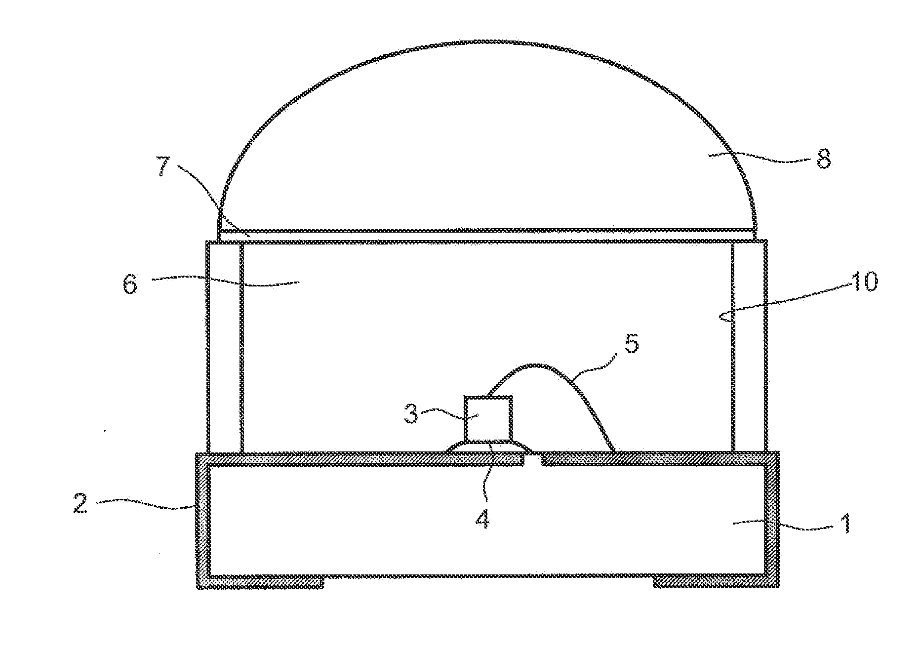
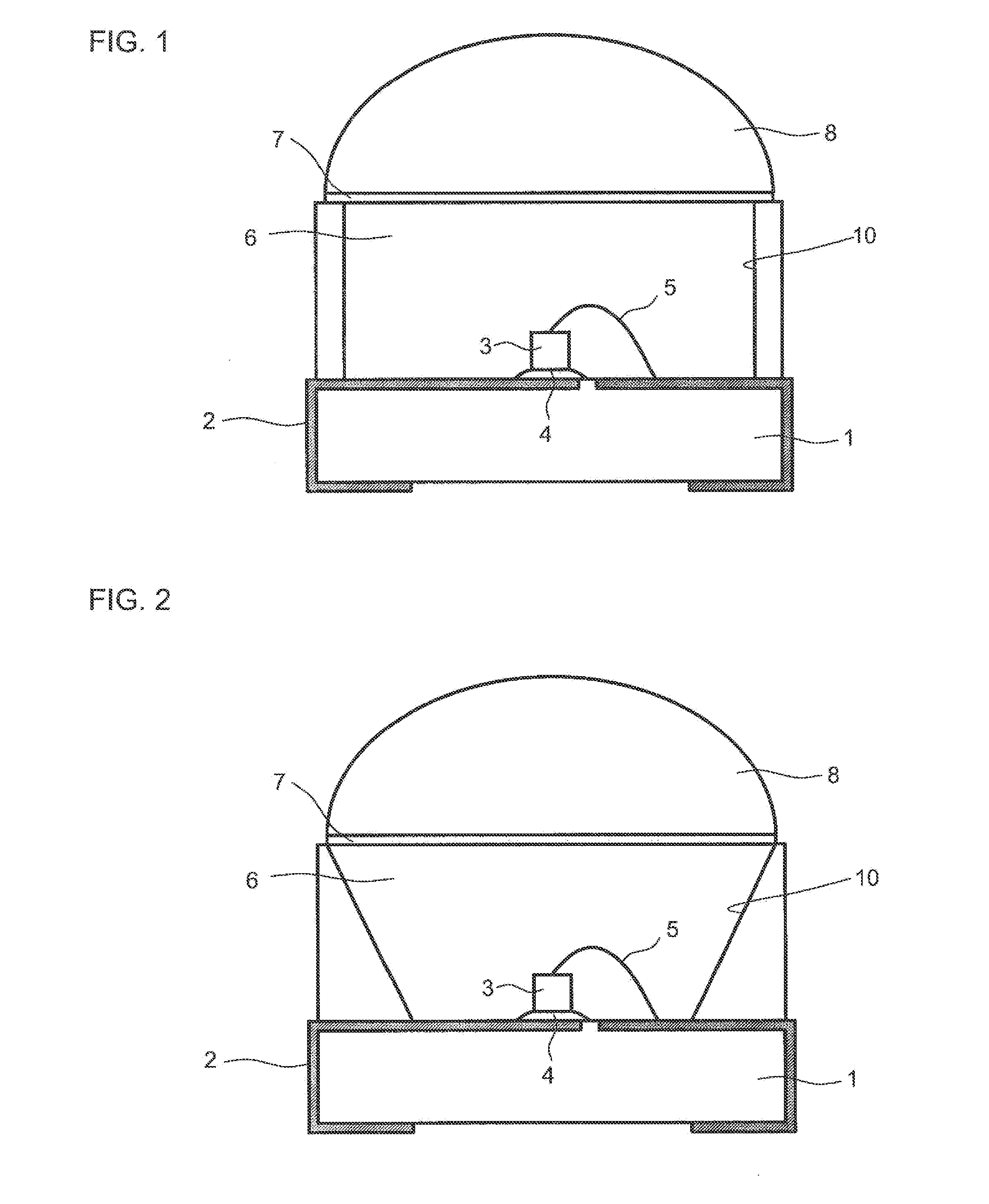
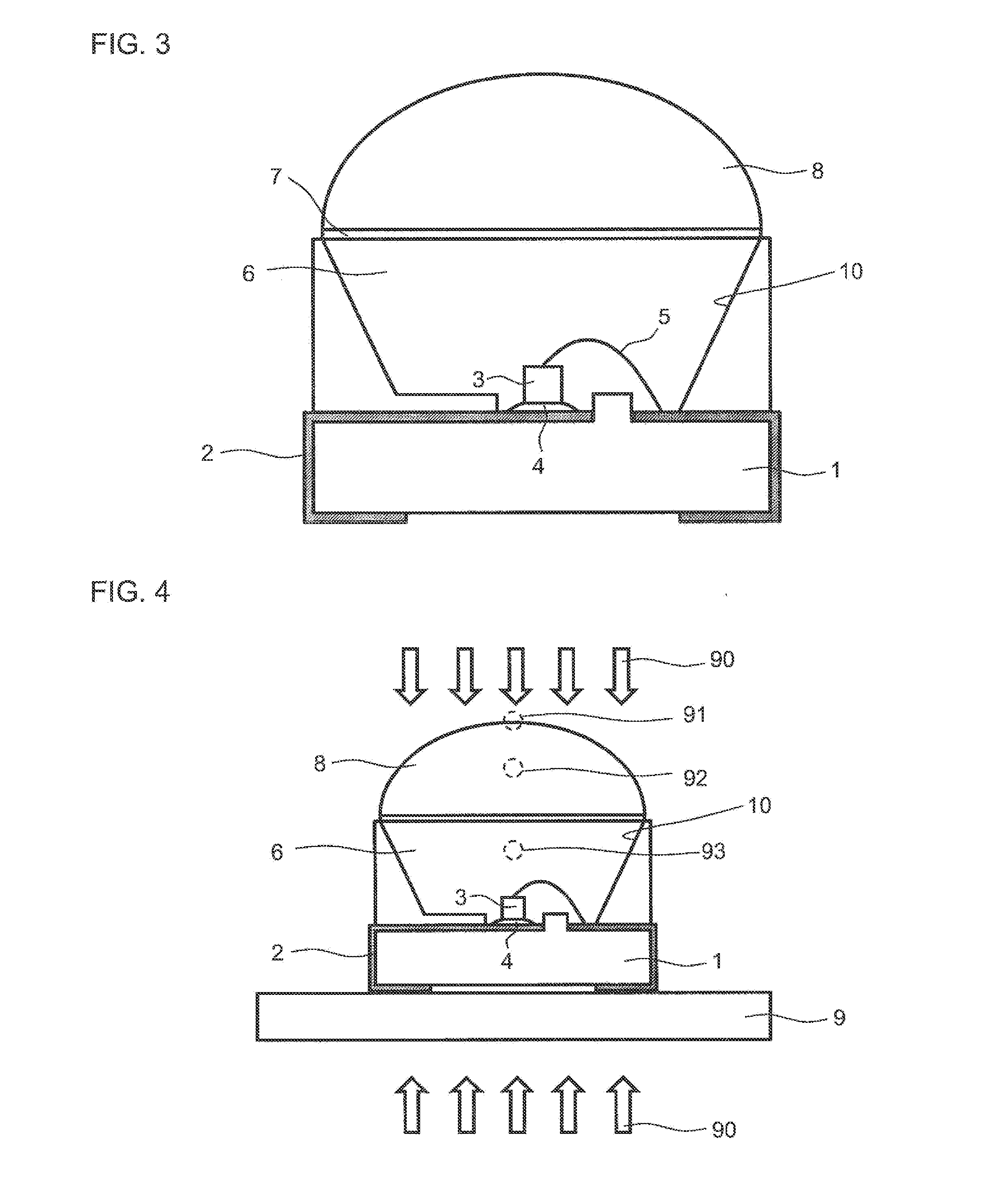
[0028]FIG. 1 shows an exemplary embodiment of an electronic component comprising a housing body 1. The housing body 1 has a depression 10, in which a semiconductor chip 3 is arranged. Purely by way of example, in the present exemplary embodiment and also in the following exemplary embodiments, the electronic component shown in each case is embodied as an optoelectronic component comprising an optoelectronic semiconductor chip and, in particular, a light-emitting semiconductor chip.

[0029]In the present exemplary embodiment, the housing body 1 comprises a thermoplastic, for example, polyphthalamide (PPA), and is shaped by means of a molding process, for example, injection molding. During the production of the housing body 1, a leadframe 2 is provided, around which the material of the housing body 1 is molded. In this case, the housing body 1 and the leadframe 2 are embodied in such a way that, as shown in FIG. 1, the electronic component is surface-mountable.

[0030]The semiconductor ch...


PUM


Abstract

An electronic component has a housing body which comprises a semiconductor chip in a recess. The semiconductor chip in the recess is embedded in a casting compound made of a first plastic material having a first glass transition temperature. A cover element made of a second plastic material having a second glass transition temperature is arranged above the recess. The second glass transition temperature is lower than the first glass transition temperature.

Description

[0001]This patent application is a national phase filing under section 371 of PCT / EP2011 / 064296, filed Aug. 19, 2011, which claims the priority of German patent application 10 2010 046 122.9, filed Sep. 21, 2010, each of which is incorporated herein by reference in its entirety.TECHNICAL FIELD[0002]An electronic component is specified.BACKGROUND[0003]If a semiconductor component such as, for instance, a light-emitting diode (LED) is fixed on a carrier such as, for instance, a printed circuit board by means of a soldering process, then the LED and its component parts are subjected to thermomechanical stresses as a result of the heating required for soldering and the subsequent cooling. If the LED has, for example, a housing comprising a plurality of different plastic parts in which a semiconductor chip is arranged, then the thermomechanical stresses in the housing can act on the semiconductor chip in such a way that the latter is detached or lifted off of a mounting area. This can le...

Claims


Application Information

Patent Timeline
Patent Type & Authority Applications(United States)
IPC IPC(8): H01L33/64
CPCH01L31/0203H01L33/56H01L33/58H01L33/641H01L2224/73265H01L2224/48091H01L2924/00014
Inventor RAMCHEN, JOHANNKEITH, CHRISTINABRAUNE, BERT
Owner OSRAM OLED
Why Eureka
Try Eureka