

Electronic package for millimeter wave semiconductor dies
a technology of semiconductor dies and electronic packaging, applied in the direction of semiconductor devices, semiconductor/solid-state device details, electrical equipment, etc., can solve the problems of increasing the size of the package, affecting the transmission of low-frequency signals to the electronic circuit board, and affecting the accuracy of millimeter wave signals, etc., to achieve effective heat dissipation and low cost
- Summary
- Abstract
- Description
- Claims
- Application Information
AI Technical Summary
Benefits of technology
Problems solved by technology
Method used
Image

Examples
embodiment
Electronic Package Embodiment
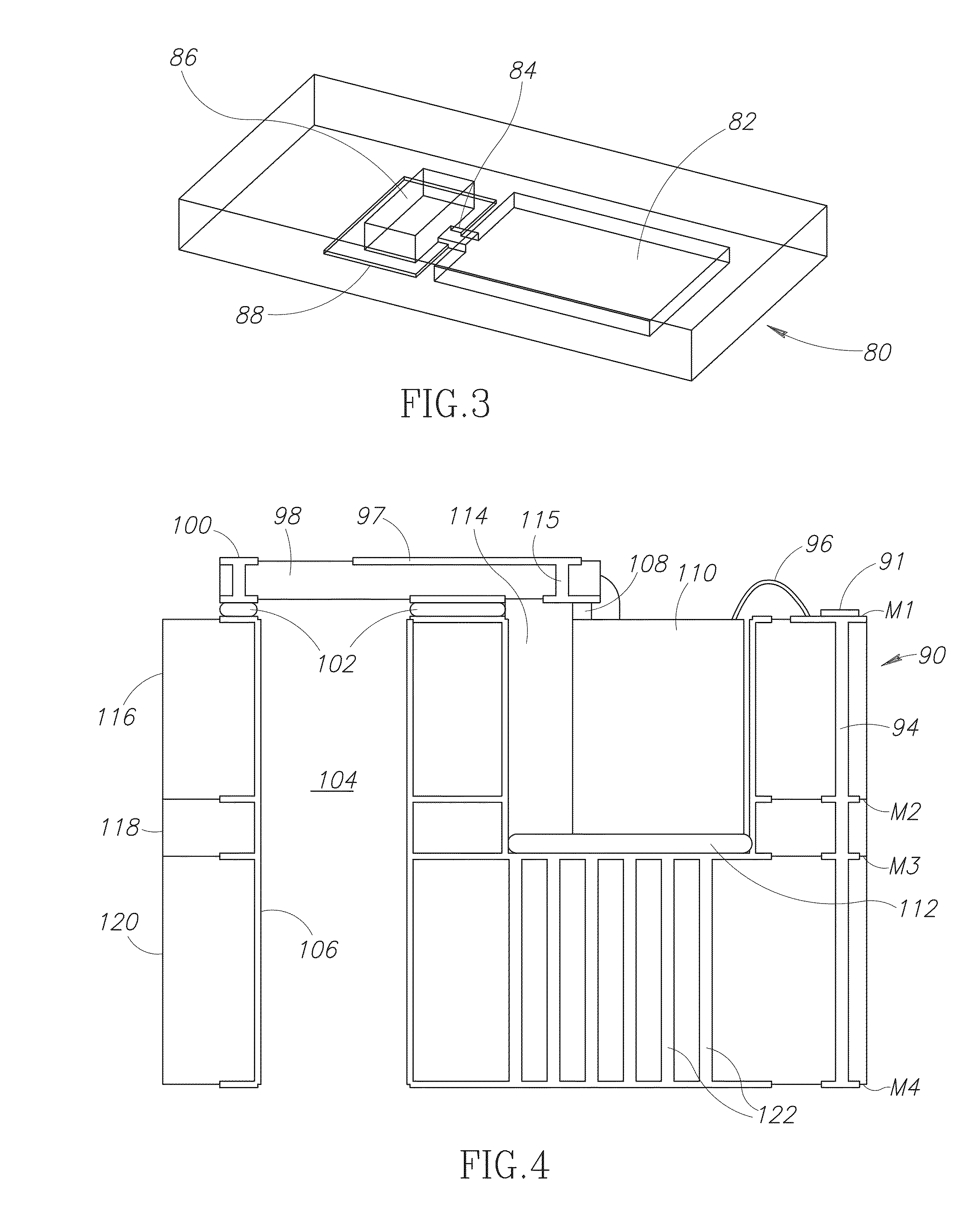
[0033]An electronic packaging system for millimeter wave semiconductor chips provides electrical connections between a millimeter wave semiconductor chip and an electric circuit board, while providing heat dissipation and a mechanical protective environment. The configuration of the package enables the use of standard reflow solder processes for attachment to a printed circuit board.
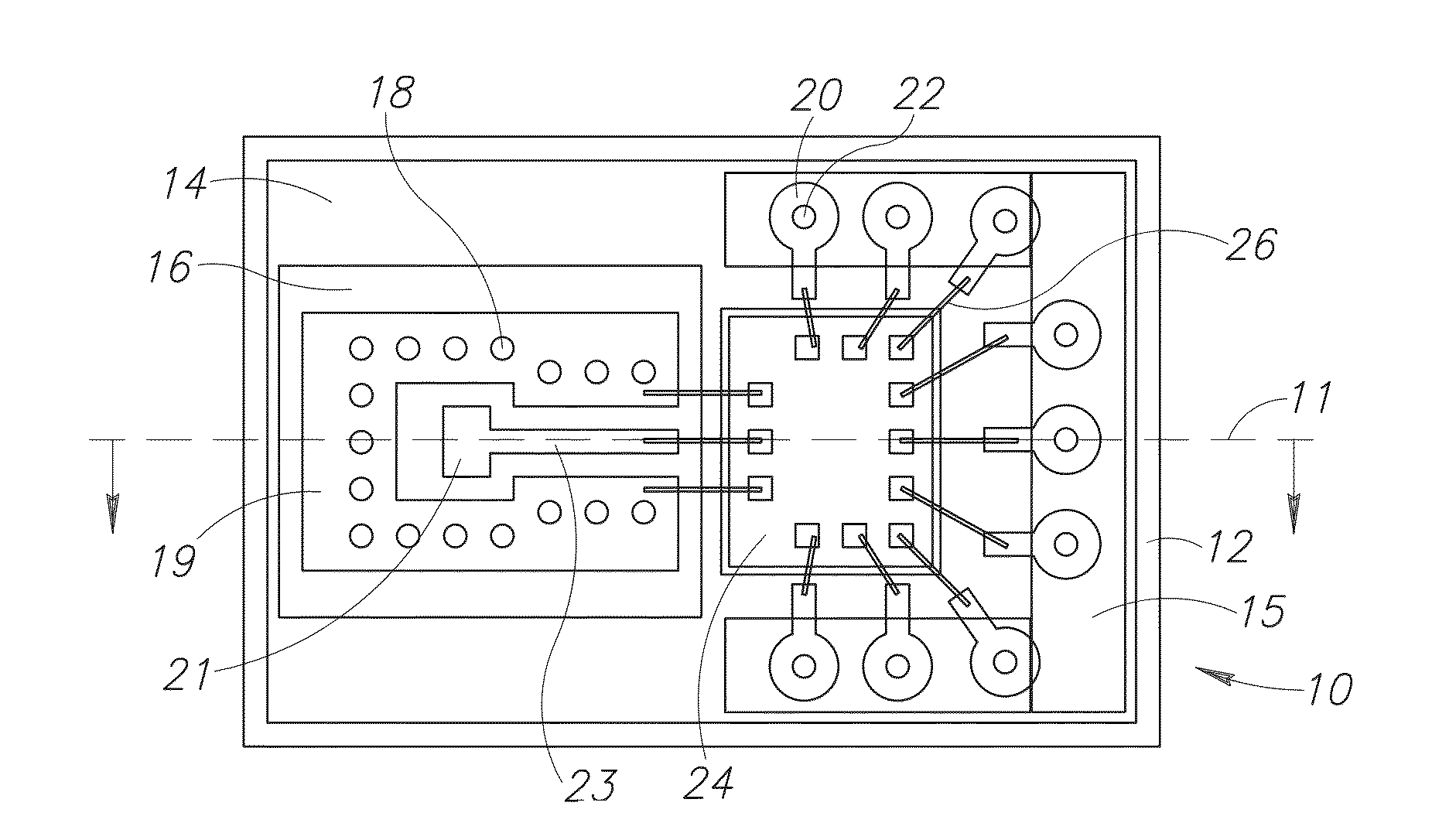
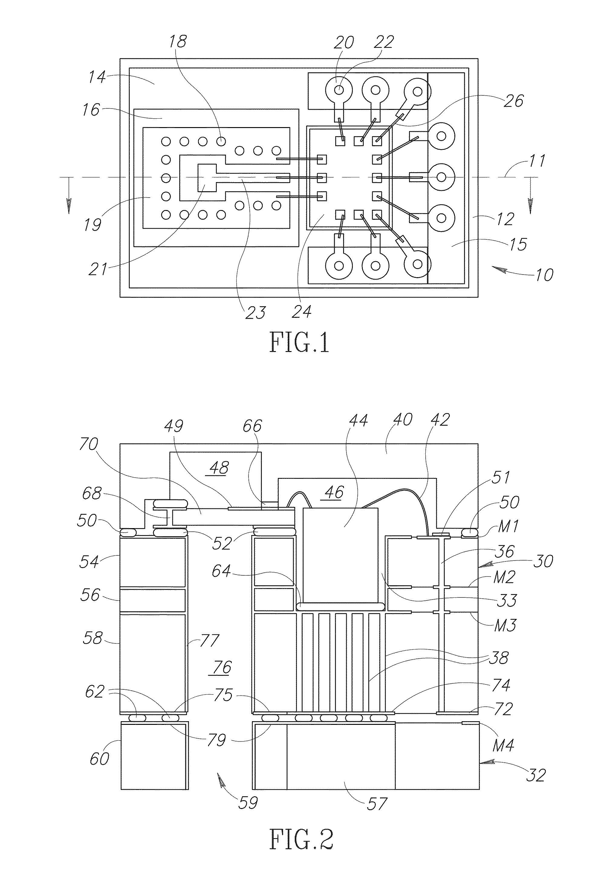
[0034]A top view of a multilayer circuit board, semiconductor chip and high frequency (HF) circuit board connected with wire bonds is shown in FIG. 1. The present invention is a combination of an SMT package, a waveguide interface and low cost production and assembly into a single device which enjoys advantages of each of the above technologies while eliminating their drawbacks.
[0035]The package, generally referenced 10, comprises a multilayer circuit board 14, constructed out of any suitable material such as FR4, semiconductor die 24 mounted on the multilayer circuit board, ...
PUM
 Abstract
Description
Claims
Application Information