Adaptive gate drive control method and circuit for composite power switch

a technology of composite power switch and gate drive control, which is applied in the direction of electronic switching, relays, pulse techniques, etc., can solve the problems of reducing the overall efficiency, affecting the reliability of the hybrid switch, and affecting the overall efficiency, so as to improve reliability, optimize the performance of the hybrid switch, and achieve high efficiency

Active Publication Date: 2013-10-03
RAYTHEON CO
View PDF3 Cites 98 Cited by
  • Summary
  • Abstract
  • Description
  • Claims
  • Application Information

AI Technical Summary

Benefits of technology

[0014]In one aspect, the invention describes a new adaptive gate drive method and circuit for a hybrid switch comprising two different power semiconductors. In one aspect of the invention improvements to switched-mode operation of a hybrid switch are proposed, through controllable gate delays and selective modes of operation for the hybrid switch. The adaptive gate drive methods and circuits in the embodiments described herein help to overcomes at least some of the limitation of conventional drive methods and circuits and allow operation at high frequencies while maintaining high efficiency, improving reliability and optimizing performance of the hybrid switch. Although the applications of the invention described herein are described mainly in terms of applicability to power transistors, specifically Metal Oxide Silicon Field Effect Transistors (MOSFETs), Bipolar Junction Transistors, and Insulated Gate Bip...

Problems solved by technology

The Conventional Hybrid Switch Approach can have some problems, however.
For example, one problem is suboptimum efficiency.
In FIG. 1, and in prior art devices, the MOSFET conduction time intervals (ΔT1 and ΔT2) are fixed, because these intervals are designed for the worst case switching times for a given IGBT and cannot accommodate changing current, temperature and device to device variations.
As a result, for most cases, the MOSFET conducts longer than necessary degrading the overall efficiency because its ON state loss is significantly higher than that of the IGBT.
Another problem is that the Static Forward and Reverse Biased Safe Operating Areas (FBSOA and RBSOA) Fixed Forward and Reverse Biased Safe Operating Areas can limit flexibility of a device to handle different types of conditions.
However, these curves strictly limit only the maximum drain to source voltage ratings.
As a result, conventional hybrid switches cannot react to changing environmental or circuit conditions such as operating at a higher junction temperature in an emergency with reduced coolant flow or providing higher current to a stalled motor.
Obviously, devices can be oversized, but it still does not prevent them from being underused in one mode of operation and overstressed in another.
A further issue is a lack of diagnostics and prognostic...

Method used


Image

  • Adaptive gate drive control method and circuit for composite power switch
  • Adaptive gate drive control method and circuit for composite power switch
  • Adaptive gate drive control method and circuit for composite power switch

Examples


Embodiment Construction

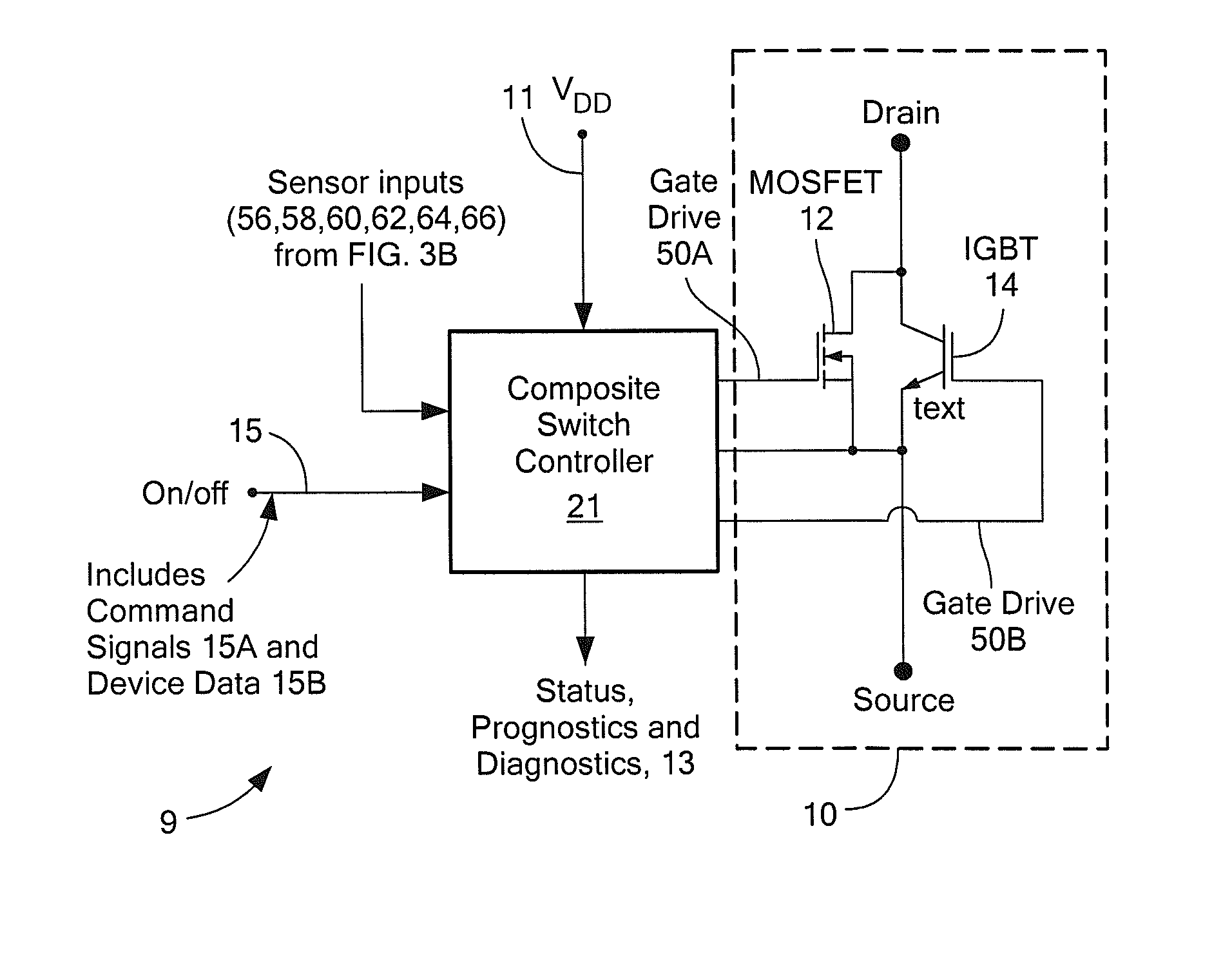
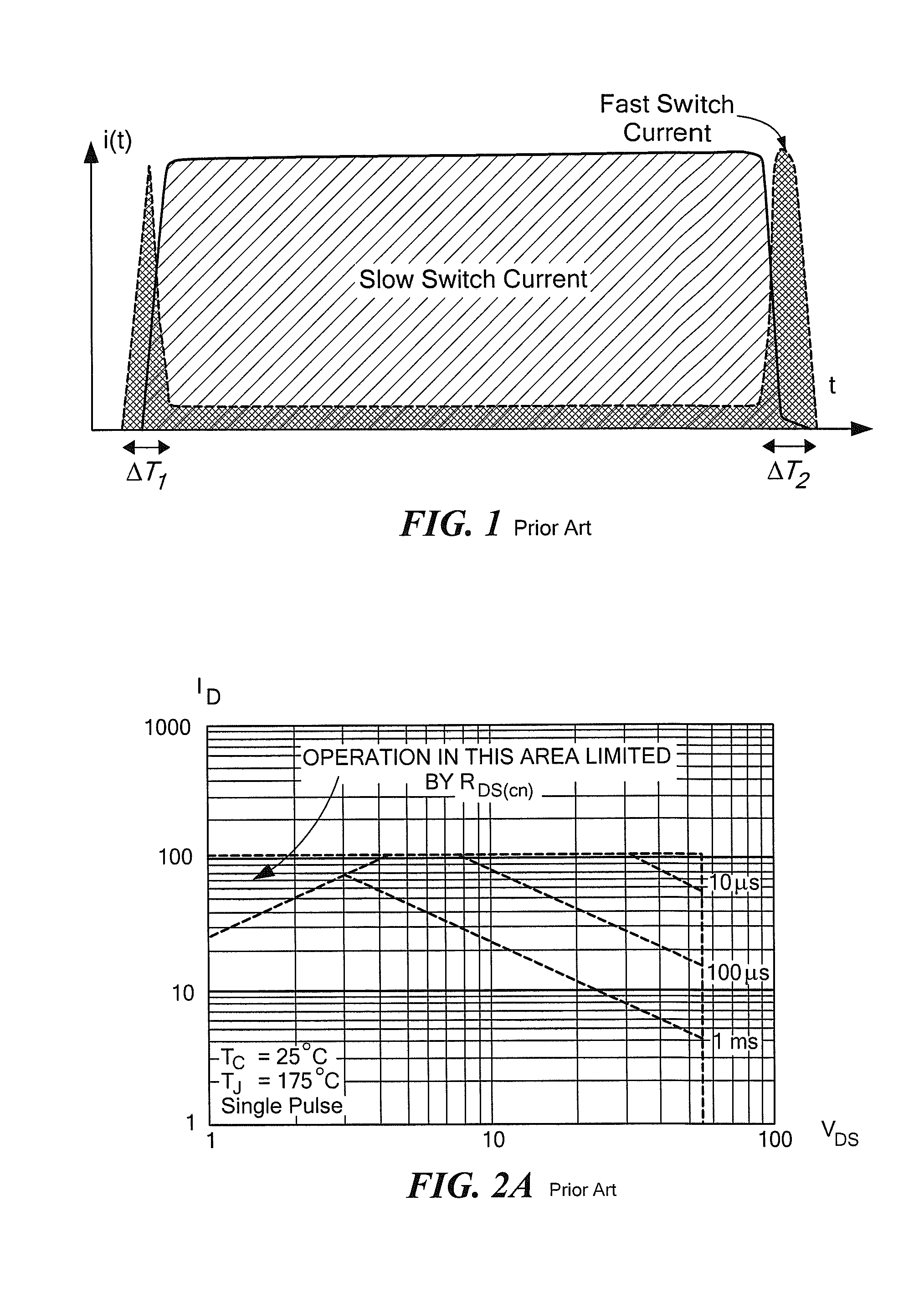
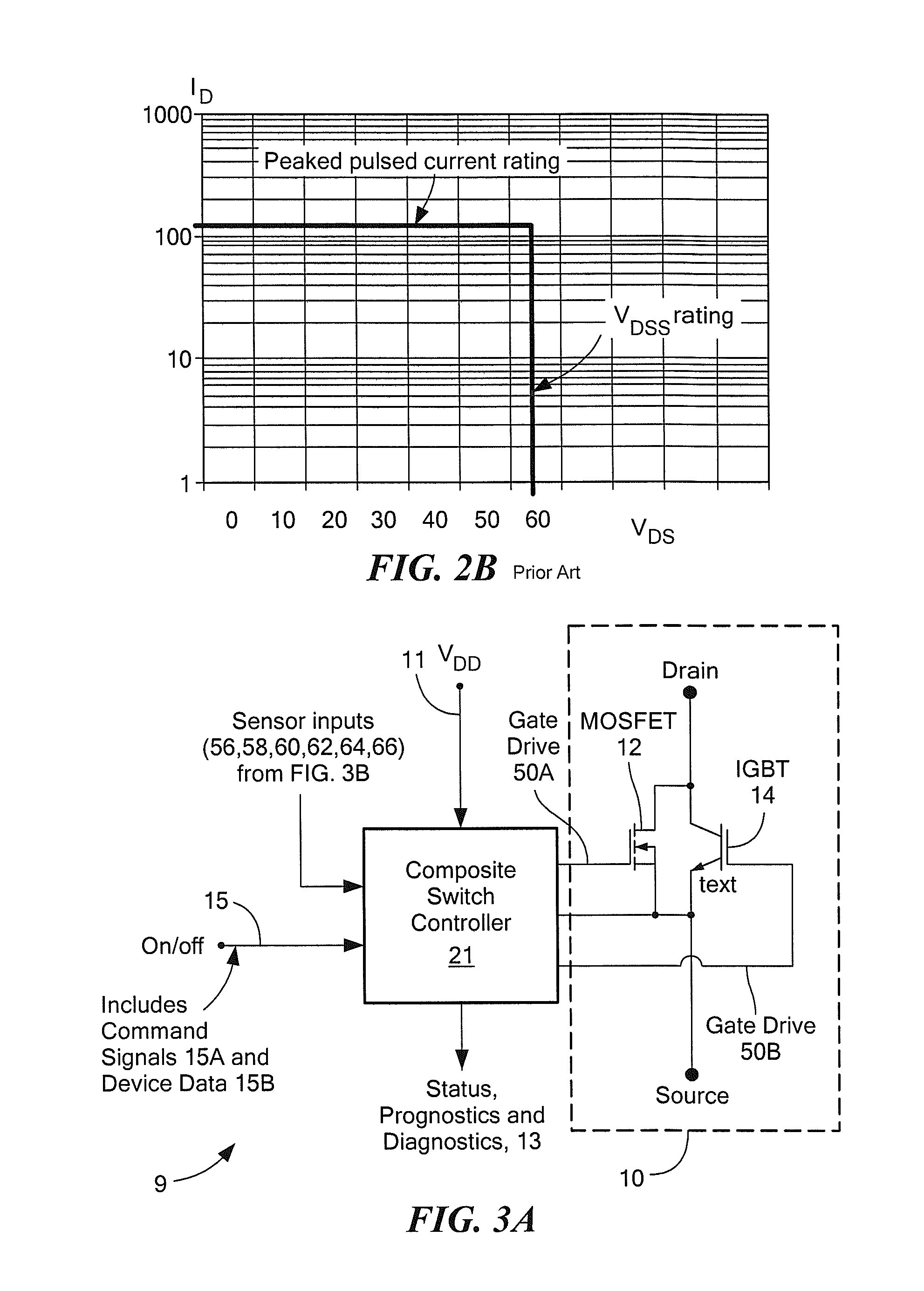
[0083]The description below explains certain features of the invention by providing examples using MOSFET and IGBT devices, properties and characteristics. It should be understood, however, that the concepts and embodiments of the invention described herein apply to many other types of semiconductor devices, including but limited to controllable semiconductors, three terminal semiconductors, and such power semiconductors as Bipolar Junction Transistors (BJTs), Insulated Gate Bipolar Transistors (IGBTs), and controllable thyristors, including Gate Turnoff (GTO) thyristors, Gate-Commutated Thyristor (GCT), Integrated Gate-Commutated Thyristor (IGCT) and Emitter Turnoff (ETO) thyristors.

[0084]FIGS. 3A and 3B show an illustrative block diagram 9 for a hybrid switch 10 with adaptive gate driver and controller 21, in accordance with one embodiment of the invention. FIG. 3A is the simplified block diagram view, and FIG. 3B is the more detailed block diagram view. In addition, in both FIG. ...


PUM


Abstract

Provided is a method of controlling a hybrid switch comprising a first individually controllable semiconductor switch operably coupled in parallel to a second individually controllable semiconductor switch. The first semiconductor switch has a faster switching speed and lower power-processing capability than the second semiconductor switch. A first reference value V1REF for a first default turn-on transition time interval ΔT1 and a second reference value V2REF for a second default turn-off transition time interval ΔT2 are accessed for the controllable hybrid switch, which is enabled and controlled so that it operates in accordance with V1REF and V2REF. The duration of the default ΔT1 and ΔT2 used to control operation of the controllable hybrid switch is dynamically adjusted to compensate for at least one of variations in a current to a load operably coupled to the controllable hybrid switch and environmental conditions at the controllable hybrid switch.

Description

CROSS REFERENCE TO RELATED APPLICATIONS[0001]Not applicableSTATEMENT REGARDING FEDERALLY SPONSORED RESEARCH[0002]Not Applicable.FIELD OF THE INVENTION[0003]Embodiments of the invention generally relate to semiconductors and systems. More particularly, the invention relates to systems, methods, and devices for operating, controlling, and monitoring power semiconductors and systems.BACKGROUND OF THE INVENTION[0004]Power semiconductor devices are well known to those of ordinary skill in the art and are commonly used for electronic power conversion, regulation, and control. As building blocks of power systems, power semiconductor devices operate in both a switching mode and a linear mode. Power semiconductors satisfy such conflicting requirements as low weight and volume, high circuit-level reliability, fault isolation, and diagnostic capabilities. Power transistors are a type of power semiconductor that is used in a variety of applications in the power range from watts to megawatts. Wh...

Claims


Application Information

Patent Timeline
IPC IPC(8): H03K17/56
CPCH02M1/08H03K17/0406H03K17/04123H02M3/33584H03K17/127H03K17/14H03K17/567H03K17/122
Inventor JACOBSON, BORIS S.JUNG, EDWARD
Owner RAYTHEON CO
Why Eureka
Try Eureka