Light emitting diode

a light-emitting diode and light-emitting technology, applied in the direction of basic electric elements, electrical equipment, semiconductor devices, etc., can solve the problems of inability to effectively achieve the radioactive recombination of electron-hole pairs and inability to evenly distribute into all quantum wells

Inactive Publication Date: 2013-10-17
IND TECH RES INST
View PDF6 Cites 4 Cited by
  • Summary
  • Abstract
  • Description
  • Claims
  • Application Information

AI Technical Summary

Benefits of technology

[0007]In an exemplary embodiment, an LED is provided. In the LED, one of the three quantum barrier layers closest to a p-type semiconductor layer has a thickness greater than thicknesses of the other two quantum barrier layers. Thereby, electron-hole pairs may be evenly distributed into the quantum barrier layers of the active layer, and luminous intensity of the LED at the 222 nm-405 nm wavelength range can be improved.

Problems solved by technology

Therefore, radiative recombination of the electron-hole pairs cannot be effectively accomplished.
Besides, since hole mobility is less than electron mobility, therefore, when holes are injected into the active layer from the p-type semiconductor layer, the holes are mostly confined in the quantum well closest to the p-type semiconductor layer and cannot be evenly distributed into all quantum wells.

Method used


Image

  • Light emitting diode
  • Light emitting diode
  • Light emitting diode

Examples


Embodiment Construction

[0024]Below, exemplary embodiments will be described in detail with reference to accompanying drawings so as to be easily realized by a person having ordinary knowledge in the art. The inventive concept may be embodied in various forms without being limited to the exemplary embodiments set forth herein. Descriptions of well-known parts are omitted for clarity, and like reference numerals refer to like elements throughout.

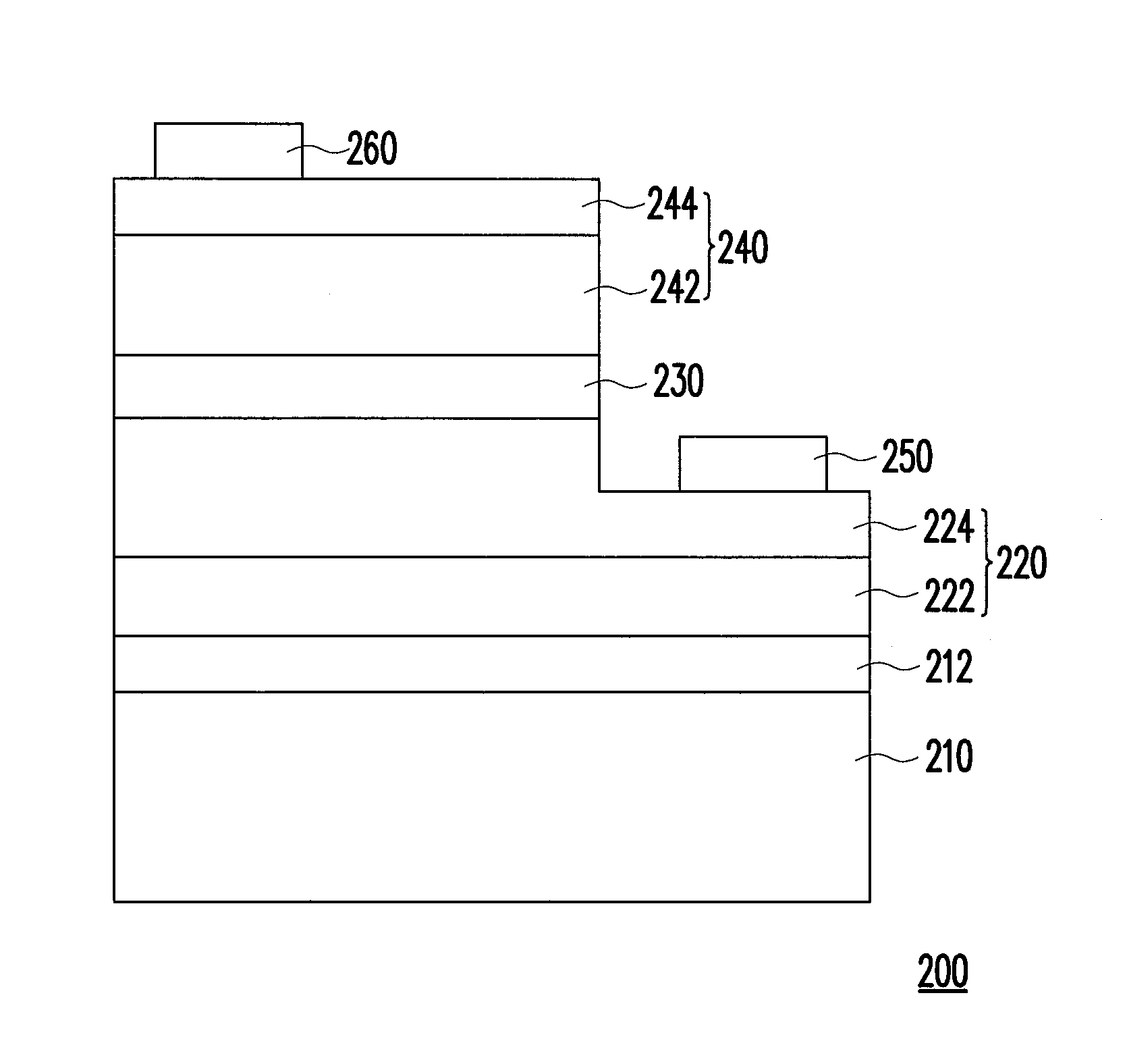
[0025]FIG. 1 is a schematic cross-sectional diagram illustrating an LED according to an exemplary embodiment.

[0026]With reference to FIG. 1, an LED 200 includes a substrate 210, an n-type semiconductor layer 220, an active layer 230, a p-type semiconductor layer 240, a first electrode 250, and a second electrode 260. The substrate 210 is, for instance, a sapphire substrate. Specifically, the stacking layers of a nitride semiconductor capping layer 212 (e.g. un-doped GaN), a n-type semiconductor layer 220, an active layer 230, the active layer 230 and the p-type semi...


PUM


Abstract

A light emitting diode includes a substrate, an n-type semiconductor layer, a p-type semiconductor layer, an active layer, a first electrode, and a second electrode. The n-type semiconductor layer is located between the substrate and the p-type semiconductor layer. The active layer is located between the n-type semiconductor layer and the p-type semiconductor layer. The wavelength of light emitted by the active layer is λ, and 222 nm≦λ≦405 nm. The active layer includes i quantum barrier layers and (i−1) quantum wells, each quantum well is located between any two quantum barrier layers, and i is an integer greater than or equal to 2. The thickness of each of the quantum barrier layers counting from the p-type semiconductor layer is T1 to Ti, and T1 is greater than T2 and T3, or T1=T2>T3, or T1>T2>T3.

Description

CROSS-REFERENCE TO RELATED APPLICATION[0001]This application claims the priority benefit of Taiwan application serial no. 101113026, filed on Apr. 12, 2012. The entirety of the above-mentioned patent application is hereby incorporated by reference herein and made a part of this specification.BACKGROUND[0002]1. Technical Field[0003]The disclosure relates to a light emitting diode (LED), and more particularly, to an LED capable of enhancing luminous intensity.[0004]2. Related Art[0005]A light emitting diode (LED) is a semiconductor device constituted mainly by group III-V compound semiconductor materials, for instance. Such semiconductor materials have a characteristic of converting electricity into light; hence, when a current is applied to the semiconductor materials, electrons therein would be combined with holes and release excessive energy in a form of light, thereby achieving an effect of luminosity.[0006]For instance, it is assumed that the LED is made of a nitride-based semico...

Claims


Application Information

Patent Timeline
Patent Type & Authority Applications(United States)
IPC IPC(8): H01L33/04
CPCH01L33/06H01L33/32
Inventor FU, YI-KENG
Owner IND TECH RES INST
Why Eureka
Try Eureka