
Semiconductor device

a technology of semiconductor devices and semiconductor devices, applied in the direction of semiconductor devices, electrical equipment, transistors, etc., can solve the problems of difficult control of circuits including such transistors, and the negative threshold voltage of transistors that are not suitable for use in semiconductor devices in integrated circuits

Active Publication Date: 2013-10-17
SEMICON ENERGY LAB CO LTD
View PDF7 Cites 66 Cited by
  • Summary
  • Abstract
  • Description
  • Claims
  • Application Information

AI Technical Summary

Benefits of technology

The present invention relates to a transistor structure and method for forming it that can achieve a normally-off transistor with a close-to-zero threshold voltage even when the transistor is a normally-on transistor. One embodiment of the transistor includes oxide semiconductor stacked layers with a thinner channel formation region that helps to suppress the shift of the threshold voltage in the negative direction. The transistor also includes a first gate electrode layer and a second gate electrode layer between which the oxide semiconductor layer including the channel formation region is sandwiched, with a bias voltage applied to one of the gate electrode layers to suppress generation of the second current and move the threshold voltage of the transistor in the positive direction. The use of a material with a large work function for the gate electrode layer also helps to move the positive ions at the interface between the oxide semiconductor layer and the gate insulating layer to the gate electrode layer side.

Problems solved by technology

A transistor having a negative threshold voltage tends to be what is called a normally-on transistor that passes a current between a source and a drain even at a gate voltage of 0 V, and a circuit including such a transistor is difficult to control.
For this reason, the transistor having the negative threshold voltage is not suited for the use in an integrated circuit of a semiconductor device.

Method used


Image

  • Semiconductor device
  • Semiconductor device
  • Semiconductor device

Examples


embodiment 1

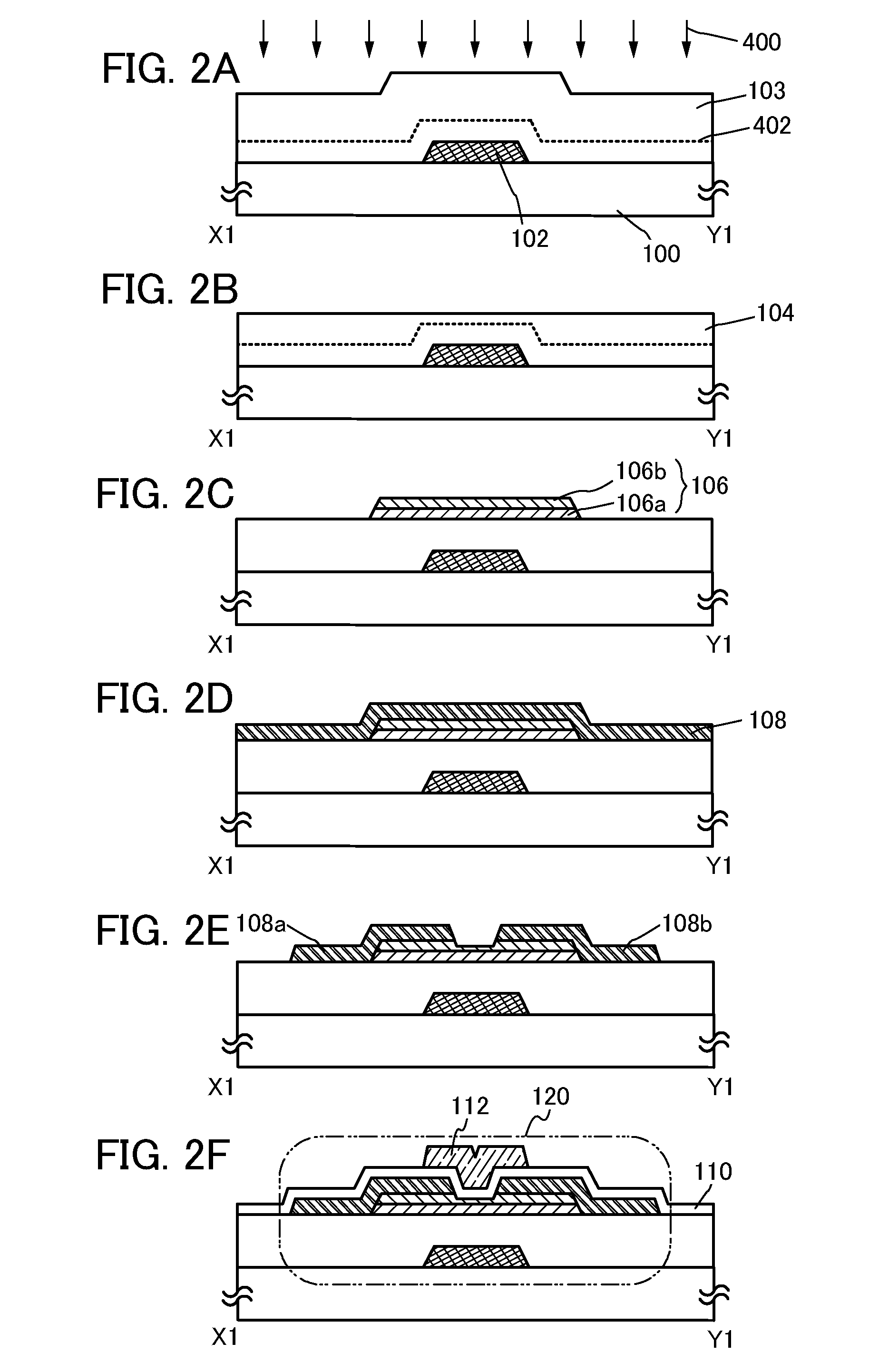
[0063]In this embodiment, one embodiment of a semiconductor device and one embodiment of a method for manufacturing the semiconductor device are described with reference to FIGS. 1A and 1B and FIGS. 2A to 2F. In this embodiment, a transistor including an oxide semiconductor stacked layers is described as an example of the semiconductor device.

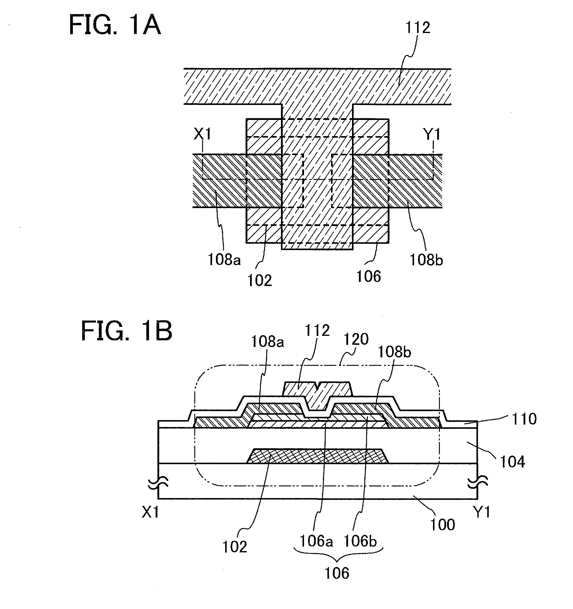
[0064]FIGS. 1A and 1B illustrate an example of a structure of a transistor 120. FIG. 1A is a plan view of the transistor 120, and FIG. 1B is a cross-sectional view taken along a chain line X1-Y1 in FIG. 1A.

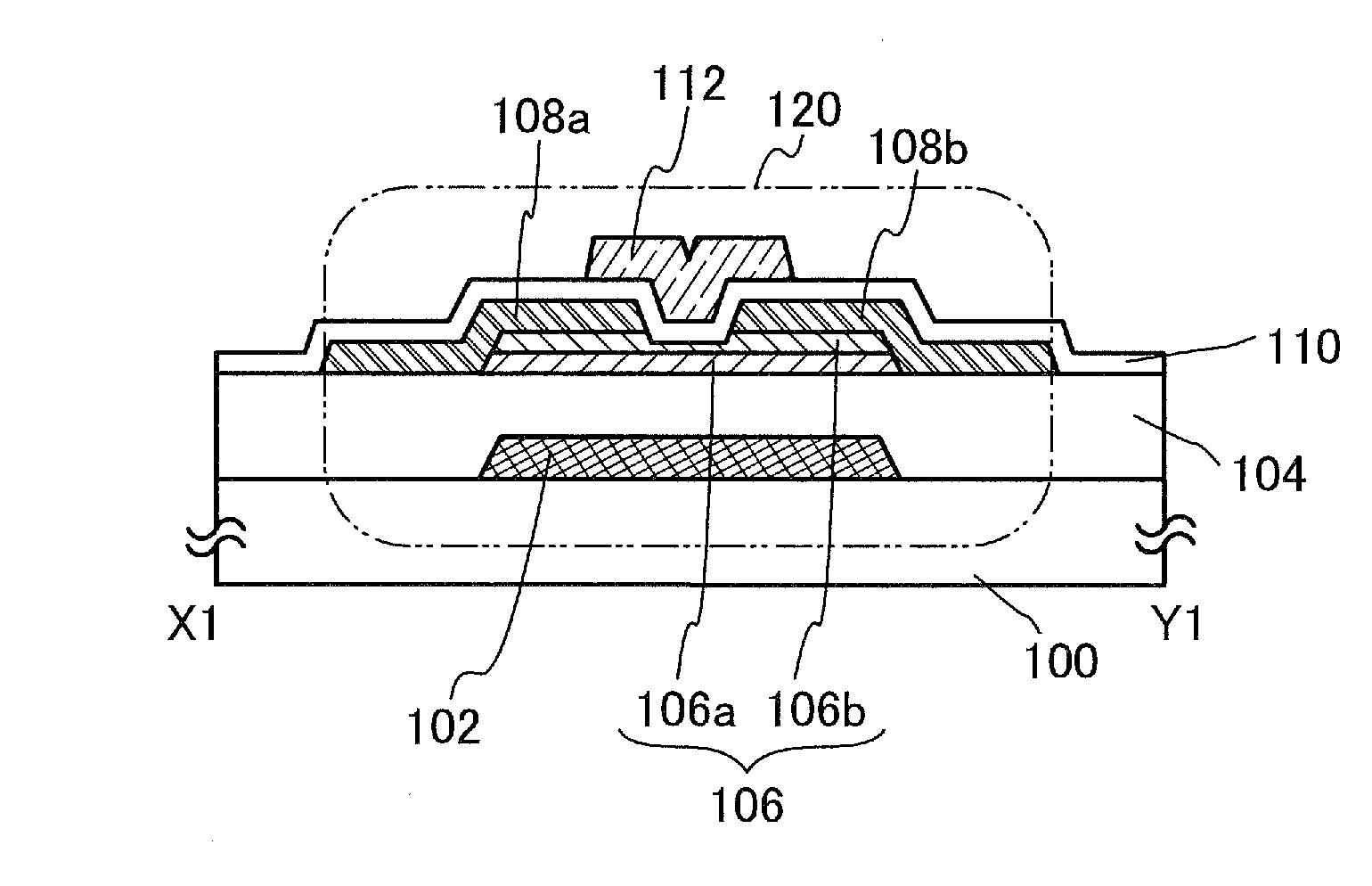
[0065]As illustrated in the cross-sectional view in the channel length direction in FIG. 1B, the transistor 120 includes, over a substrate 100 having an insulating surface, a gate electrode layer 102, an insulating layer 104, an oxide semiconductor stacked layers 106 including an oxide semiconductor layer 106a and an oxide semiconductor layer 106b, a source electrode layer 108a, a drain electrode layer 108b, an insulating layer 110, and a gat...

embodiment 2

[0150]In this embodiment, as an example of a semiconductor device which includes the transistor described in Embodiment 1, a semiconductor device which can hold stored data even when not powered and which has an unlimited number of write cycles will be described with reference to drawings.

[0151]FIGS. 3A and 3B illustrate one example of a structure of the semiconductor device. FIG. 3A is a cross-sectional view of the semiconductor device, and FIG. 3B is a circuit diagram of the semiconductor device.

[0152]The semiconductor device illustrated in FIG. 3A includes a transistor 160 including a first semiconductor material in a lower portion, and a transistor 162 including a second semiconductor material in an upper portion. As the transistor 162, the transistor of one embodiment of the present invention described in Embodiment 1 can be employed.

[0153]Here, the first semiconductor material and the second semiconductor material are preferably materials having different band gaps. For exampl...

embodiment 3

[0184]In this embodiment, a semiconductor device including the transistor described in Embodiment 1, which can hold stored data even when not powered, which does not have a limitation on the number of write cycles, and which has a structure different from the structure described in Embodiment 2 will be described with reference to FIGS. 4A and 4B.

[0185]FIG. 4A illustrates an example of a circuit configuration of the semiconductor device, and FIG. 4B is a conceptual diagram illustrating an example of the semiconductor device. First, the semiconductor device illustrated in FIG. 4A will be described, and then, the semiconductor device illustrated in FIG. 4B will be described.

[0186]In the semiconductor device illustrated in FIG. 4A, a bit line BL is electrically connected to the source electrode layer or the drain electrode layer of the transistor 162, a word line WL is electrically connected to the gate electrode layer of the transistor 162, and the source electrode layer or the drain e...


PUM


Abstract

A transistor includes oxide semiconductor stacked layers between a first gate electrode layer and a second gate electrode layer through an insulating layer interposed between the first gate electrode layer and the oxide semiconductor stacked layers and an insulating layer interposed between the second gate electrode layer and the oxide semiconductor stacked layers. The thickness of a channel formation region is smaller than the other regions in the oxide semiconductor stacked layers. Further in this transistor, one of the gate electrode layers is provided as what is called a back gate for controlling the threshold voltage. Controlling the potential applied to the back gate enables control of the threshold voltage of the transistor, which makes it easy to maintain the normally-off characteristics of the transistor.

Description

TECHNICAL FIELD[0001]The invention disclosed in this specification relates to a semiconductor device and a method for manufacturing the semiconductor device.[0002]In this specification and the like, a semiconductor device refers to all types of devices that can function by utilizing semiconductor characteristics; an electro-optical device, a light-emitting display device, a semiconductor circuit, and an electronic device are all semiconductor devices.BACKGROUND ART[0003]A technique for forming a transistor by using a semiconductor thin film formed over a substrate having an insulating surface has attracted attention. Such a transistor is applied to a wide range of semiconductor electronic devices such as an integrated circuit (IC) and an image display device (also simply referred to as display device). A silicon-based semiconductor material is widely known as a material for a semiconductor thin film applicable to the transistor. As another material, an oxide semiconductor has been a...

Claims


Application Information

Patent Timeline
Patent Type & Authority Applications(United States)
IPC IPC(8): H01L29/786
CPCH01L29/7869H01L27/1225H01L27/1255H01L29/7831
Inventor YAMAZAKI, SHUNPEIMATSUBAYASHI, DAISUKEMURAYAMA, KEISUKE
Owner SEMICON ENERGY LAB CO LTD
Learn More