Deposition mask and method for manufacturing organic light emitting display using the same

a technology of light-emitting display and mask, which is applied in the manufacture of electrode systems, discharge tubes luminescnet screens, electrode systems, etc., can solve the problems of damage to organic films, negative influence of outgasing on organic films, and photolithography that exposes organic films to moisture during resist exfoliation or etching

Active Publication Date: 2006-01-19
SAMSUNG DISPLAY CO LTD
View PDF7 Cites 34 Cited by
  • Summary
  • Abstract
  • Description
  • Claims
  • Application Information

AI Technical Summary

Benefits of technology

[0016] The present invention provides a deposition mask and a method for manufacturing an organic light emitting display (OLED) using the same capable of preventing an organic film from being destroyed or chemical transition from occurring due to contact of sealed portion of the mask and an EML already deposited during a deposition process of an organic EML.
[0017] The present invention may inure various advantages. First, the indented portion of the mask may not touch already deposited organic EML, thereby preserving the organic EML. Second, it may be possible to prevent chemical transition from occurring at the organic EML. Third, the deposition mask can be obtained in a simple method and additional processes may not be required for the OLED manufacturing process. Thus, productivity can be improved.

Problems solved by technology

This is because the organic film may be very vulnerable to moisture and thus may require thorough isolation from moisture during and after the manufacturing process.
Therefore, photolithography that exposes the organic film to moisture during a resist exfoliation or etching may not be appropriate for patterning the organic film and the second electrode.
This can damage the organic film.
However, even in that case, a blocked-off portion of the mask may touch the spacer and thus small fragments (and fragments of the spacer) and outgasing may have a negative influence on the organic film.

Method used


Image

  • Deposition mask and method for manufacturing organic light emitting display using the same
  • Deposition mask and method for manufacturing organic light emitting display using the same
  • Deposition mask and method for manufacturing organic light emitting display using the same

Examples


Embodiment Construction

[0030] The present invention will now be described more fully with reference to the accompanying drawings, in which exemplary embodiments of the invention are shown.

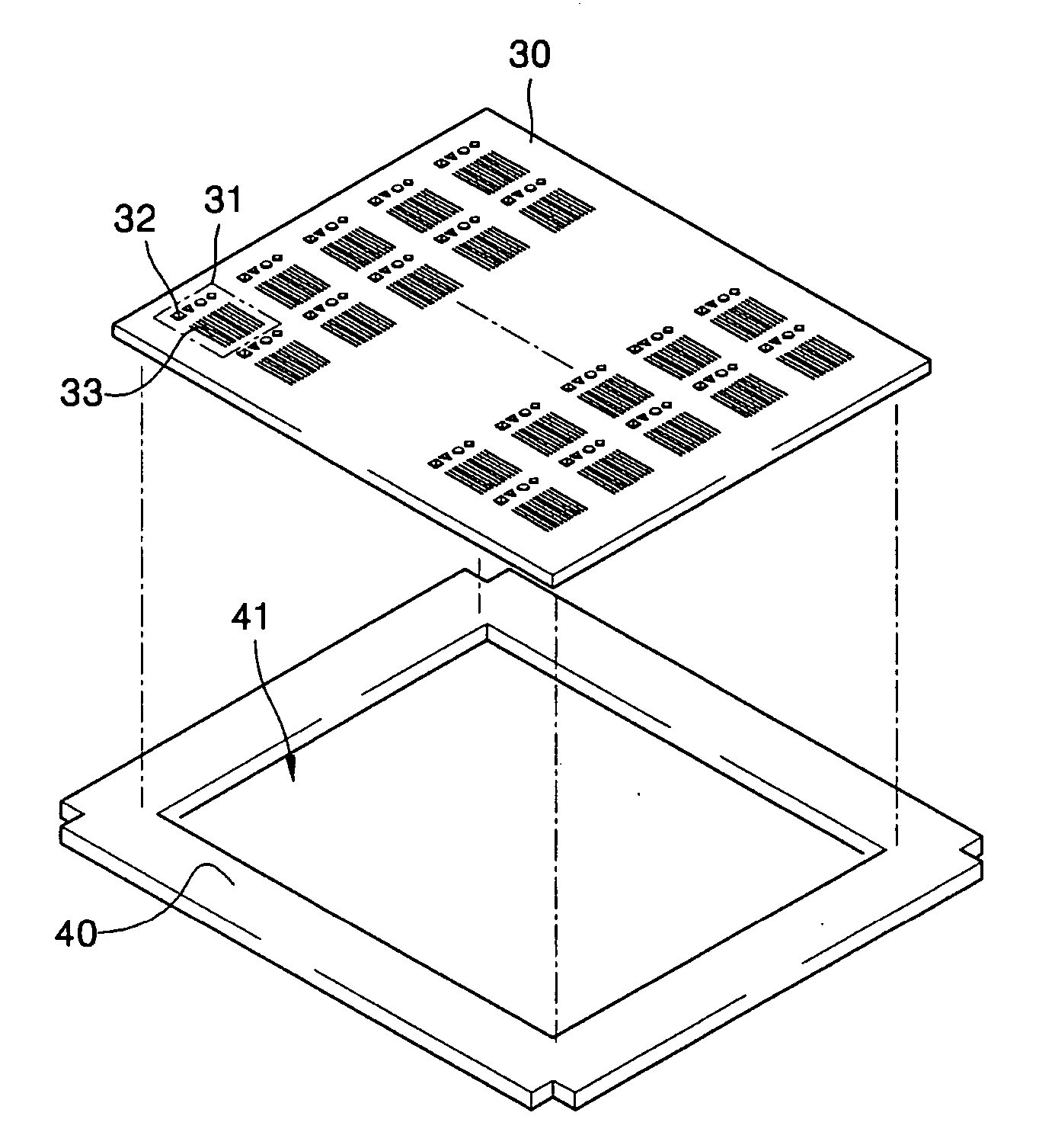
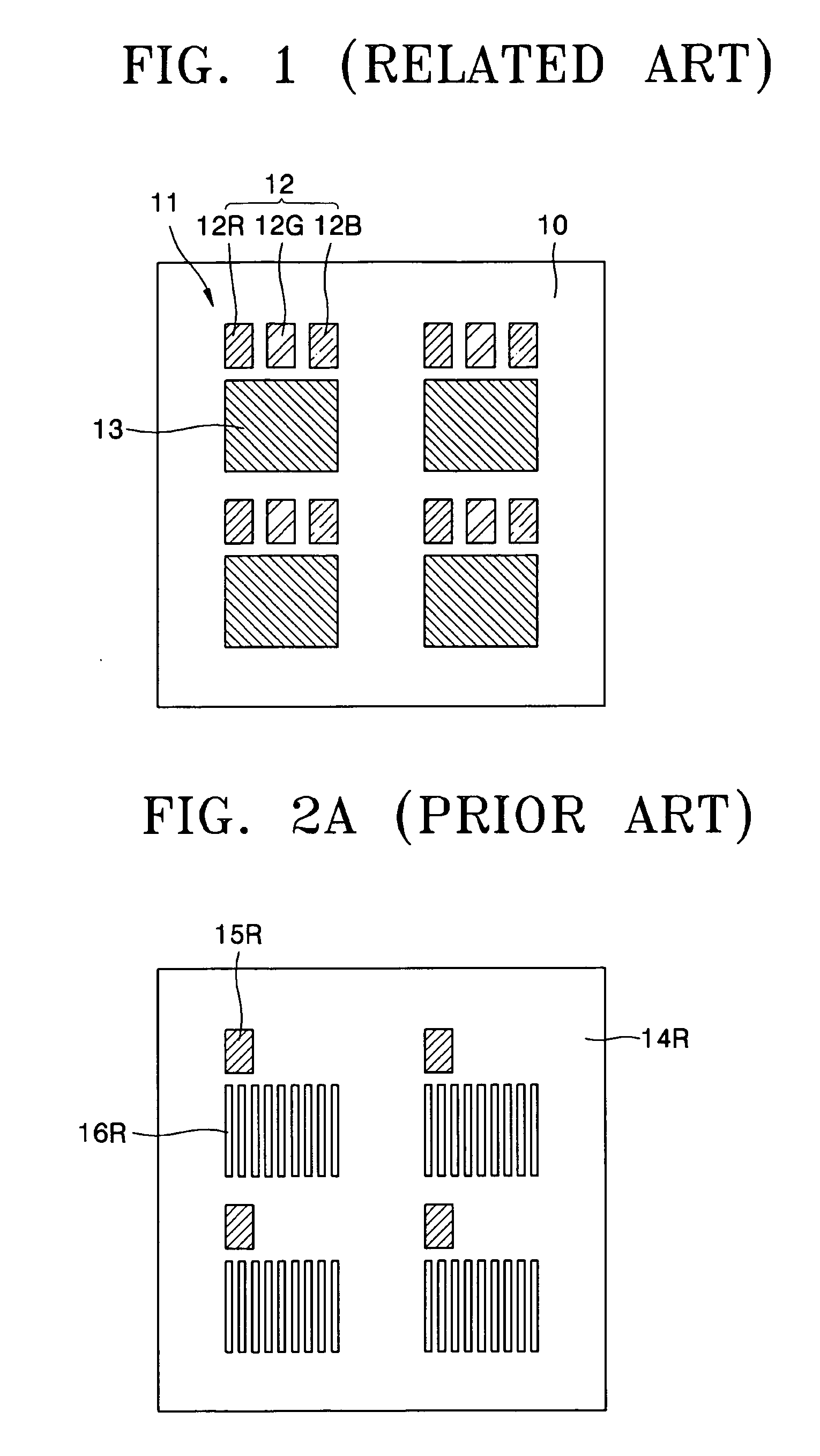
[0031] The present invention can be used to manufacture an OLED as illustrated in FIG. 1. As described above, the substrate 10 of FIG. 1 has four panel regions but the present invention is not necessarily limited to this. The present invention can have a plurality of panel regions and have the OLED formed on the respective panel regions.

[0032] As described above, the OLED of the respective panels 11 can include an icon part 12 and a main image part 13. The icon part 12 can include a red emission region 12R, a green emission region 12G, and a blue emission region 12B. The main image part 13 can have a red sub-pixel, a green sub-pixel, and a blue sub-pixel so as to realize full color.

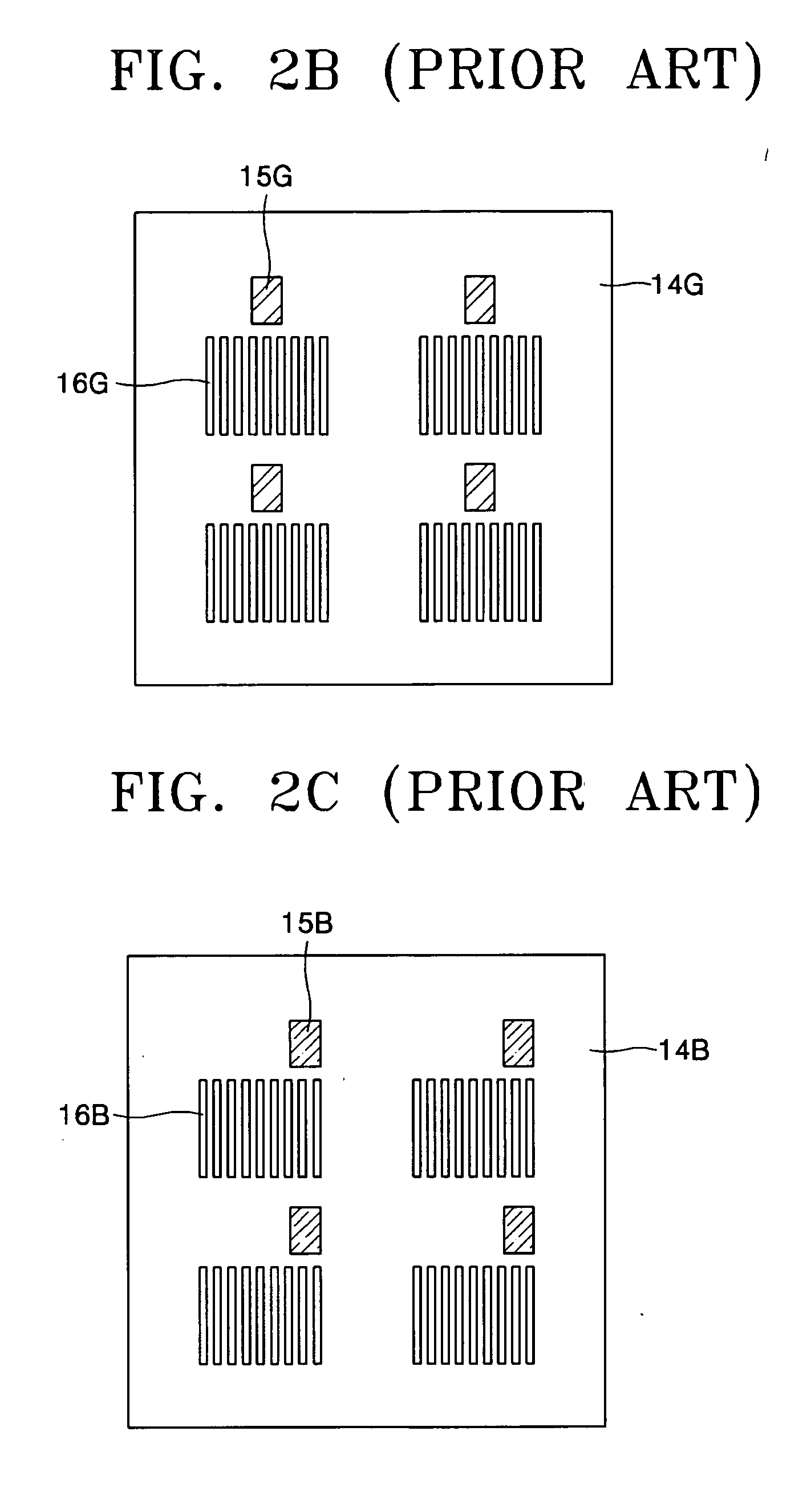
[0033] At this point, the icon part 12 and the main image part 13 can have the structure illustrated in FIG. 3. This structure is further ...


PUM

PropertyMeasurementUnit
thicknessaaaaaaaaaa
depthaaaaaaaaaa
coloraaaaaaaaaa

Abstract

A deposition mask and a method for manufacturing an organic light emitting display (OLED) using the same are provided. The deposition mask is intended for preventing an organic film from being damaged due to touching of a blocked-off portion of the mask to an emission layer (EML), or chemical transition from being generated at the organic film. For that purpose, the deposition mask stuck to a substrate of the OLED to deposit an organic EML includes an opening and an indentation. The opening is opened so as to deposit the organic EML. The indentation is indented a predetermined depth from a plane facing the substrate.

Description

CROSS-REFERENCE TO RELATED PATENT APPLICATION [0001] This application claims the benefit of Korean Patent Application No. 10-2004-0055072, filed on Jul. 15, 2004, which is incorporated herein in its entirety by reference. BACKGROUND OF THE INVENTION [0002] 1. Field of the Invention [0003] The present invention relates to a deposition mask and a method for manufacturing an organic light emitting display (OLED) using the deposition mask. More particularly, the invention relates to a deposition mask that can be used in depositing an organic emission layer (EML) and a method for manufacturing the OLED with such an EML. [0004] 2. Description of the Related Art [0005] An OLED typically includes a first electrode formed in a predetermined pattern on a transparent insulation substrate, an organic film formed by, for example, vacuum deposition on the first electrode, and a second electrode formed on an upper surface of the organic film. [0006] The first electrode is generally made of a trans...

Claims


Application Information

Patent Timeline
Patent Type & Authority Applications(United States)
IPC IPC(8): H01J9/02H01J1/62
CPCH01L27/3211H01L51/56H01L51/0011C23C14/042H10K59/35H10K71/166H10K71/00H05B33/10
Inventor KANG, CHANG-HOKIM, TAE-SEUNGHONG, JAE-MIN
Owner SAMSUNG DISPLAY CO LTD
Why Eureka
Try Eureka