Supercharge Your Innovation With Domain-Expert AI Agents!

Method for input/output design of chip

a chip and input/output technology, applied in the field of input/output (io) design of chips, can solve the problems of increasing the cost of the chip, ssn, and the magnitude of the nois

Active Publication Date: 2013-10-24
GLOBAL UNICHIP CORPORATION +1
View PDF6 Cites 1 Cited by
  • Summary
  • Abstract
  • Description
  • Claims
  • Application Information

AI Technical Summary

Benefits of technology

The invention relates to a method for designing an input / output (IO) chip's signal pins. The method involves setting parameters for each signal pin and checking whether the pins' operation timing meets their associated timingu specifications. The method iterates until the pins' operation timing does not violate the timingu specifications. This allows the chip design to be optimized for better performance. The process involves performing a setting step, a timing verification step, and a re-verification step, with the driving parameters being changed accordingly. The invention helps to improve the performance and reliability of the chip's signal pins.

Problems solved by technology

When many signal IO cells simultaneously drive their output signals to switch (referred to as simultaneous switching output, SSO), impacts to the power voltage VddIO and / or the ground voltage Vss additively accumulate and consequently induce simultaneous switching noise (SSN).
Therefore, when multiple signal IO cells simultaneously drive signal switching and induce SSN, magnitude of the noise relates to equivalent (parasite) circuits of the circuit board, the chip package, the IO supply pads and the power stripes.
Increasing quantity of the IO supply pads / cells in a chip can effectively reduce inductance of the equivalent circuits; however, an excessively incremented number of IO supply cells / pins will expand overall layout area of the chip and thus increase cost of the chip.
Because the driving factors are fractional, the SDF also includes a fraction portion which is rounded to obtain integer quantities of IO supply cells; hence, IO design of the prior art suffers from over-design, which means that the IO design tends to adopt excessive numbers of IO supply pins, and thus impacts prevalence of chip by increased total pin count, overall layout area and cost of the chip.
Furthermore, the prior art only considers numbers of IO supply cells, while geometric locations of signal IO cells and IO supply cells are left unconsidered.
However, because the prior art ignores such factors, there is no way to know preferable locations for placing IO supply cells, and it is difficult to achieve better trade-off between SSN suppression and pin count reduction.
However, the prior art does not consider parasite effects of chip package and / or circuit board, thus IC designer of prior art tends to adopt signal IO cells of higher driving strength (and / or slew rate), such that timing specifications of signal IO cells are satisfied by expanded driving margin.
In other words, due to lack of integrated consideration, IC designer of prior art needs to over-design driving strength.
That is, a driving factor only considers signal IO cells of the same type; if the IO design adopts a mixed arrangement including signal IO cells of different types, correctness of driving factor is affected; consequently, the prior art can not assure correctness of whole IO design.

Method used


Image

  • Method for input/output design of chip
  • Method for input/output design of chip
  • Method for input/output design of chip

Examples


Embodiment Construction

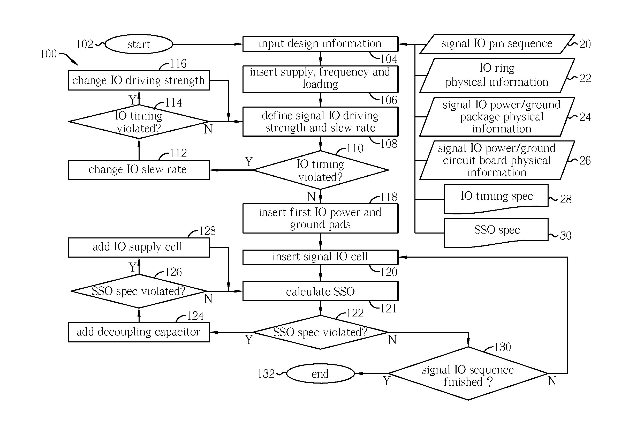
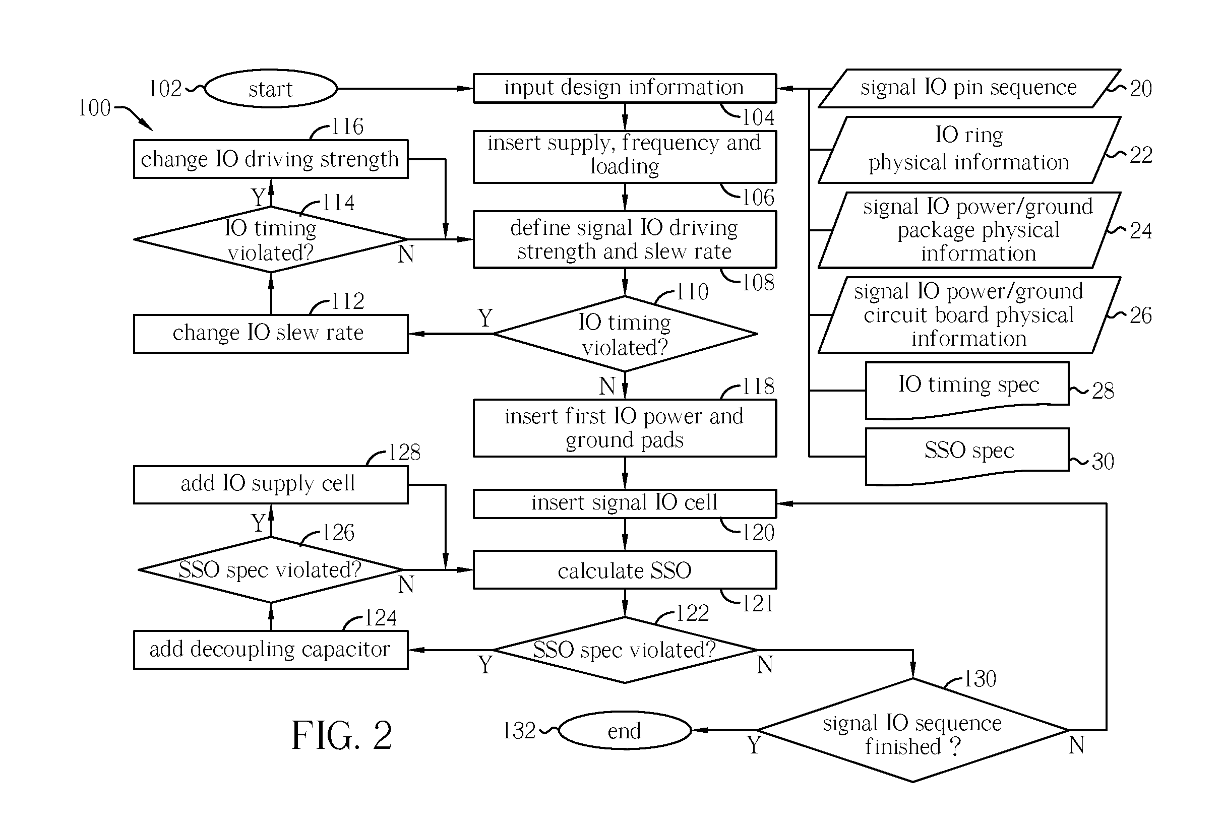
[0028]Please refer to FIG. 2 illustrating a flow 100 according to an embodiment of the invention, the flow 100 implements IO design technology of the invention to provide an IO design of a chip. Major steps of the flow 100 are described as follows.

[0029]Step 102: start the flow 100.

[0030]Step 104: input design information. For example, design information 20 to 30 listed in FIG. 2 can be included in IO design consideration of the invention. The design information 20, 22, 24, 26, 28 and 30 can respectively be a signal IO pin sequence, IO ring physical information, signal IO power / ground package physical information, signal IO power / ground circuit board physical information, IO timing specification and SSO specification (checking rules).

[0031]The signal IO pin sequence of the design information 20 records signal IO pins required to be implemented in the IO design, including number of the signal IO pins, logic arrangement order of the signal IO pins, and / or required minimal driving stre...


PUM


Abstract

Method for input / output (IO) design of a chip, including: according to a signal IO pin sequence and associated driving parameters, sequentially placing a signal IO cell in the IO design associated with each of the signal IO pins; after a signal IO cell is placed, performing a simultaneous switching output (SSO) verification step according to physical layout parameters and locations of the signal IO cells placed in the IO design, so as to check whether an SSO specification is violated; if not violated, continuing to place a signal IO cell of a next signal IO pin; if violated, including a decoupling capacitor, an IO power cell and / or an IO ground cell in the IO design.

Description

[0001]This application claims the benefit of Taiwan Patent Application No. 101113853, filed Apr. 18, 2012, the subject matter of which is incorporated herein by reference.FIELD OF THE INVENTION[0002]The present invention relates to a method for input / output (IO) design of chip, and more particularly, to a chip IO design method which integrates information about geometric locations of signal IO cells during consideration of simultaneous switching output (SSO).BACKGROUND OF THE INVENTION[0003]Chips (including dice, integrated circuits and / or system-on-chips, etc.) form one of the most important hardware foundations of modern information society, chip designers are also eagerly developing better strategy, flow and technology of chip design not only to satisfy basic demands and specifications of customers but also to minimize chip layout area for cost reduction.[0004]Please refer to FIG. 1 illustrating an embodiment of a chip 10. The chip 10 includes a core circuit 14 and an IO interfac...

Claims


Application Information

Patent Timeline
Patent Type & Authority Applications(United States)
IPC IPC(8): G06F17/50
CPCG06F17/5081G06F2113/18G06F30/39G06F2119/06G06F30/398
Inventor CHEN, SHI-HAOTSAI, TSUNG-YINGHUANG, CHAO-YEN
Owner GLOBAL UNICHIP CORPORATION
Features
  • R&D
  • Intellectual Property
  • Life Sciences
  • Materials
  • Tech Scout
  • Unparalleled Data Quality
  • Higher Quality Content
  • 60% Fewer Hallucinations
Learn More