

RE-PROGRAMMABLE ANTIFUSE FPGA UTILIZING RESISTIVE CeRAM ELEMENTS
a ceram element and antifuse technology, applied in logic circuits, pulse techniques, instruments using specific components, etc., can solve the problems of low resistance change memory, low resistance change yield, and inability to achieve 100% yield
- Summary
- Abstract
- Description
- Claims
- Application Information
AI Technical Summary
Benefits of technology
Problems solved by technology
Method used
Image

Examples
embodiment 100
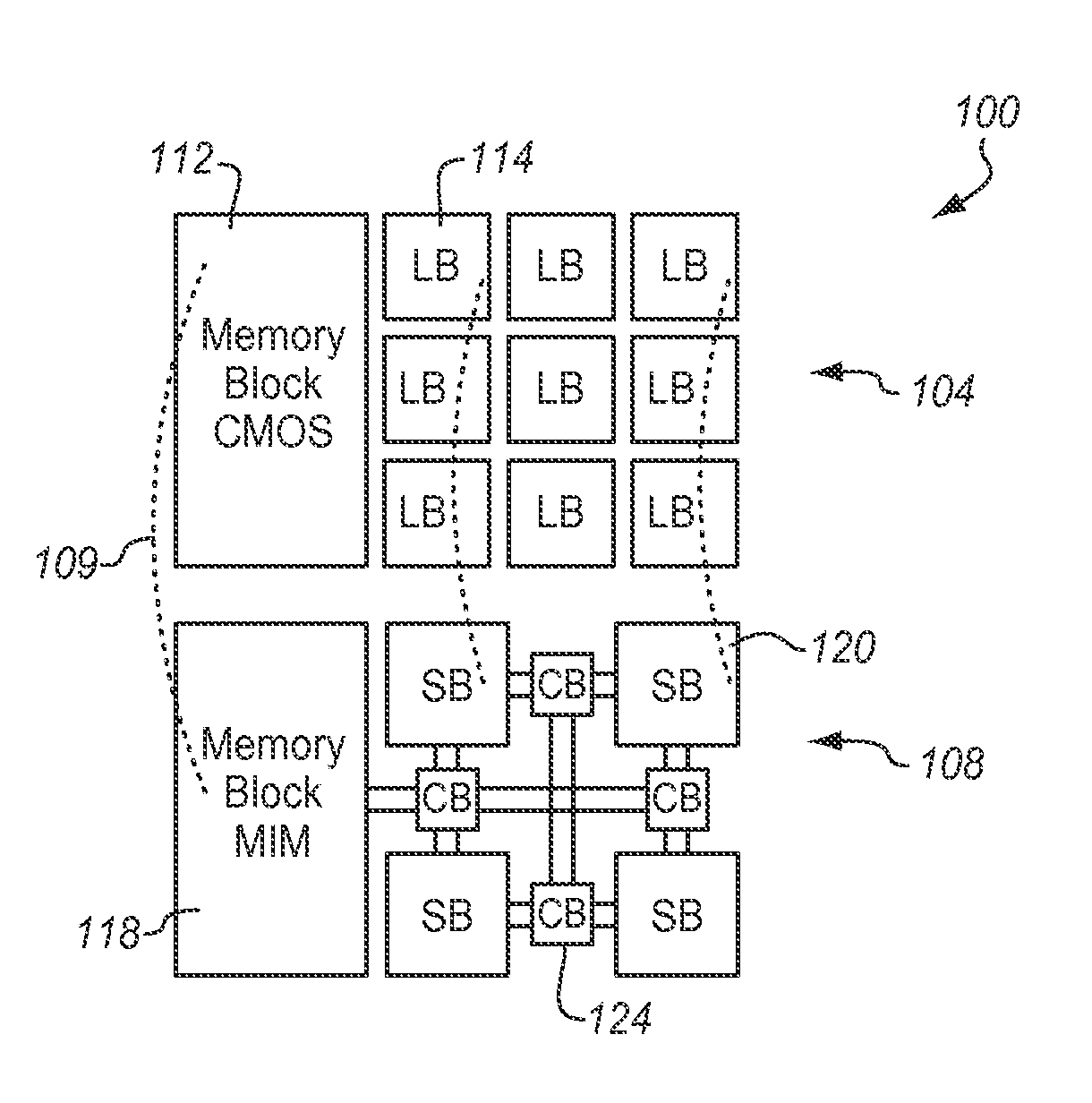
[0022]FIG. 1 shows a block level representation of one embodiment of a memory 100. Memory embodiment 100 includes a CeRAM module 108 and a logic module 104. The CeRAM module 108 lies on top of the logic module 104 as shown by the dotted lines 109. In one embodiment, logic module 104 includes logic blocks (LB), such as 114, and CMOS memory block 112. CeRAM module 108 includes metal / insulator / metal (MIM) memory block 118, switch blocks (SB), such as 120, and connection blocks (CB), such as 124. A CeRAM memory block, such as 118, in a 1T1 R (1-transistor, 1-resistor) circuit configuration, which is roughly the size of one transistor, for the memory blocks as a replacement for traditional 6T (6-transistor) SRAM could yield a density enhancement of roughly five to six times the existing architecture. As will be seen in more detail below, one embodiment of the structure comprises a field programmable gate array (FPGA). In one embodiment, the routing resources of an FPGA consist of switch ...
embodiment 140
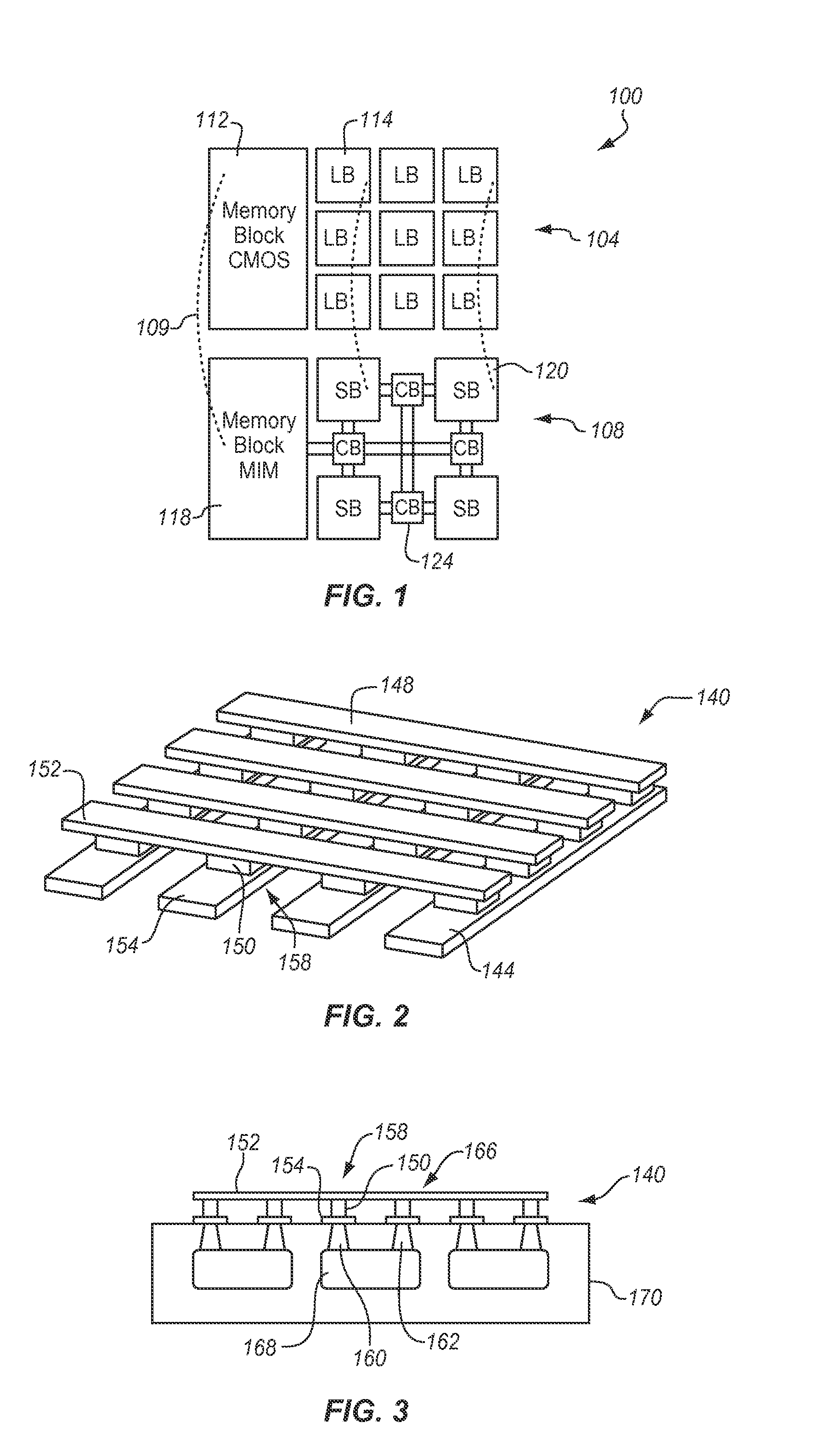
[0023]FIG. 2 illustrates an embodiment 140 of a crossbar structure. This embodiment includes metal lines, such as 148, placed perpendicular to and on top of metal lines, such as 144. In this disclosure, the term “metal” when used in the context of an integrated circuit may mean a metal material, but, as is traditional in the art, may also mean a conductive material, such as polysilicon. A resistive memory element, such as 158, is formed at the juncture of each upper conductor and lower conductor by a CeRAM layer, such as 150, disposed between upper conductor 152 and lower conductor 154.
[0024]FIG. 3 is a cross-sectional view of an embodiment of a crossbar structure 140 integrated with a CMOS logic layer 170. Each CeRAM resistive cell, such as 158, is connected to a CMOS device, such as 160, by a plug, such as 160. In this embodiment, two plugs, such as 160 and 162, connect a pair of CeRAM cells, 158 and 166, to the CMOS device 168.
II. CeRAM Switch
[0025]In one embodiment, CeRAM is a r...
embodiment 650
[0038]FIG. 13 show a simplified cross-sectional view illustrating an embodiment 650 of a CeRAM element 655 incorporated into a gate-source / base-emitter connection 688 of an active CMOS resistor configuration. Cell 650 is formed on a semiconductor 652, and includes CeRAM resistive switching element 655, transistor 666, and connection 688. Transistor 666 comprises gate 670, oxide layer 672, and source / drains emitters 674 and 676 with channel 680 between them. CeRAM element 655 includes bottom electrode 668 which has an upturned contact portion 680 and a post 689 which contacts one source / drain emitter 676 of transistor 666. CeRAM 688 also includes top electrode 662 with an extension 684 over transistor 666 that extends to a downward leg 685 which forms a contact to transistor gate 670. A plug 690 makes contact with source / drain emitter 674. Electrical wiring terminals 690, 692, and 693 apply power to cell 600.
[0039]Because of the low voltage levels (Vsig≈200-300 mV), the logic blocks ...
PUM
 Abstract
Description
Claims
Application Information