
Semiconductor device and manufacturing method thereof

a technology of semiconductors and manufacturing methods, applied in the direction of transistors, television systems, radio-controlled devices, etc., can solve the problems of inability to hold charge for a long time, loss of original data, and significant leakage of charg

Active Publication Date: 2013-11-14
SEMICON ENERGY LAB CO LTD
View PDF1 Cites 9 Cited by
  • Summary
  • Abstract
  • Description
  • Claims
  • Application Information

AI Technical Summary

Benefits of technology

The patent text describes a technology for controlling the behavior of a photodiode and the formation of an oxide semiconductor layer. The text references several techniques and methods for controlling the photodiode, but notes that none of them have addressed the issue of dark current. The use of a mechanical shutter or a new switching element has increased costs and complexity. The transistor technology described in the text also discusses the use of an oxide semiconductor layer to control charge accumulation and prevent leakage of charge from the accumulation portion. Overall, the patent provides a solution for minimizing charge leakage and allowing for image capturing without distortion.

Problems solved by technology

When this charge holding period gets longer, charge flows out by leakage current and the like of a transistor forming a pixel, so that original data is lost.
In particular, there were problems that the leakage of charge becomes significant and charge cannot be held for a long period of time when the off-state current of the transistor is high.
Therefore, in the techniques disclosed in the above-described patent documents, behavior of a photodiode is controlled by any method; however, the countermeasure against dark current of a photodiode has not been made.
In addition, by addition of a mechanical shutter or of a new switching element, there was a problem in high cost and a complicated control.

Method used


Image

  • Semiconductor device and manufacturing method thereof
  • Semiconductor device and manufacturing method thereof
  • Semiconductor device and manufacturing method thereof

Examples


embodiment 1

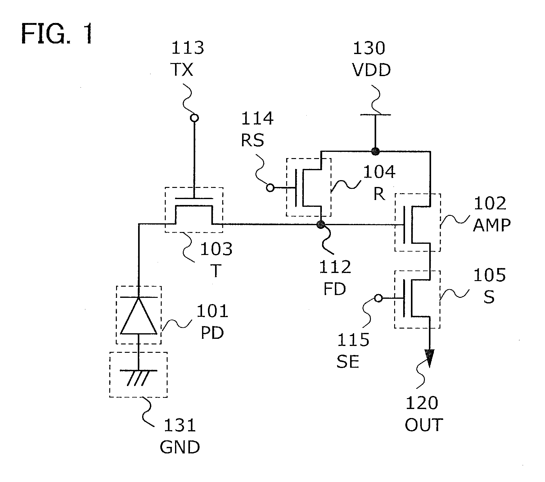
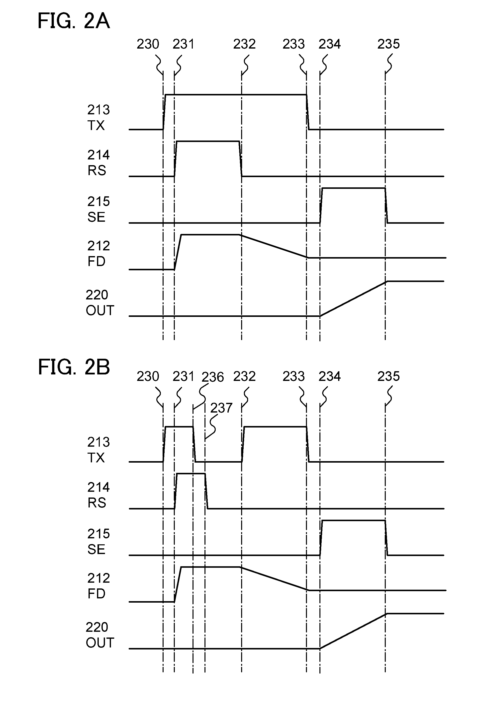
[0069]In this embodiment, a semiconductor device which is one embodiment of the present invention will be described with reference to drawings. FIG. 1 is an example of a circuit configuration of a pixel in an image sensor.

[0070]The pixel in the image sensor includes a photodiode 101 (PD), an amplifying transistor 102 (AMP), a charge accumulation control transistor 103 (T), a reset transistor 104 (R), and a selection transistor 105 (S).

[0071]Next, functions and arrangement of elements and wirings are described.

[0072]The photodiode 101 generates current in accordance with the amount of light incident on the pixel. The amplifying transistor 102 outputs a signal which corresponds to a potential of a signal charge accumulation portion 112 (FD). The charge accumulation control transistor 103 controls charge accumulation in the signal charge accumulation portion 112 performed by the photodiode 101. The reset transistor 104 controls the initialization of the potential of the signal charge a...

embodiment 2

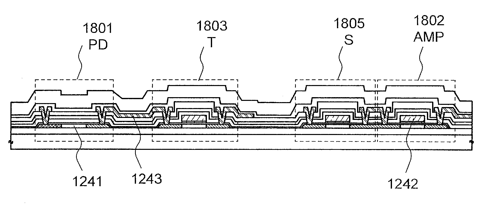
[0155]In this embodiment, a layout of a pixel circuit of a semiconductor device in one embodiment of the present invention will be described.

[0156]As an example of the case where the pixel circuit of FIG. 8 is actually formed, the top view of the layout of a pixel circuit is illustrated in FIG. 11. Note that all the transistors used for the pixel circuit of FIG. 8 are formed using a silicon semiconductor.

[0157]The pixel circuit illustrated in FIG. 11 is formed with a pin photodiode 1801, an amplifying transistor 1802, a charge accumulation control transistor 1803, a reset transistor 1804, a selection transistor 1805, a charge accumulation control signal line 1813, a reset signal line 1814, a selection signal line 1815, an output signal line 1820, a power supply line 1830, and a ground potential line 1831. Layers illustrated in the view are an i-type silicon semiconductor layer 1241, a gate wiring layer 1242, a wiring layer 1243, an n-type silicon semiconductor layer 1244, and a p-ty...

embodiment 3

[0174]In this embodiment, a structure of a pixel circuit of a semiconductor device which is one embodiment of the present invention will be described.

[0175]In one embodiment of the present invention, various structures can be used for the pixel circuit of the semiconductor device. Although an example based on the pixel circuit configuration illustrated in FIG. 1 is used for description in Embodiments 1 and 2, another pixel circuit configuration is described in this embodiment.

[0176]Note that transistors and wirings in this embodiment are named for convenience. Any of names is acceptable as long as functions of the transistors and the wirings are described.

[0177]FIG. 18 is a pixel circuit configuration of four transistors, which is similar to that in FIG. 1. A pixel circuit is formed with a photodiode 1601, an amplifying transistor 1602, a charge accumulation control transistor 1603, a reset transistor 1604, and a selection transistor 1605. The circuit configuration of FIG. 18 is dif...


PUM


Abstract

In a CMOS image sensor in which a plurality of pixels is arranged in a matrix, a transistor in which a channel formation region includes an oxide semiconductor is used for each of a charge accumulation control transistor and a reset transistor which are in a pixel portion. After a reset operation of the signal charge accumulation portion is performed in all the pixels arranged in the matrix, a charge accumulation operation by the photodiode is performed in all the pixels, and a read operation of a signal from the pixel is performed per row. Accordingly, an image can be taken without a distortion.

Description

TECHNICAL FIELD[0001]One embodiment of the present invention relates to a semiconductor device in which pixels each provided with a photosensor are arranged in a matrix and to a driving method of the semiconductor device. Further, one embodiment of the present invention relates to an electronic device including the semiconductor device.[0002]Note that the semiconductor device in this specification refers to all devices that can function by utilizing semiconductor characteristics, and electro-optic devices, semiconductor circuits, and electronic devices are all semiconductor devices.BACKGROUND ART[0003]As a semiconductor device in which pixels each provided with a photosensor are arranged in a matrix, an image sensor is known. The image sensors are provided in many portable devices such as a digital camera or a cellular phone as imaging elements. In recent years, the definition of imaging has been increased, the portable devices have been downsized, and power consumption has been red...

Claims


Application Information

Patent Timeline
Patent Type & Authority Applications(United States)
IPC IPC(8): H01L27/146H04N25/00
CPCH01L27/14603H04N5/361H01L27/14643H01L27/14632H01L27/14616H01L27/14636H01L29/7869H04N25/63H01L31/1055H04N25/75H04N25/76
Inventor KUROKAWA, YOSHIYUKIIKEDA, TAKAYUKITAMURA, HIKARUKOZUMA, MUNEHIROIKEDA, MASATAKAAOKI, TAKESHI
Owner SEMICON ENERGY LAB CO LTD
Learn More