Single metal damascene structure and method of forming the same

a single metal damascene and metal damascene technology, applied in the direction of semiconductor devices, semiconductor device details, electrical apparatus, etc., can solve the problems of front-end performance degradation, reduced contact resistance, increased resistance of tungsten plugs, etc., to reduce contact resistance, prevent metal from diffusing, and enhance device reliability

Inactive Publication Date: 2013-11-14
UNITED MICROELECTRONICS CORP
View PDF3 Cites 7 Cited by
  • Summary
  • Abstract
  • Description
  • Claims
  • Application Information

AI Technical Summary

Benefits of technology

[0007]The present invention provides a single metal damascene structure to reduce the contact resistance, prevent the metal from diffusing and enhance the device reliability.

Problems solved by technology

With minimization of the device, the resistance of the tungsten plug is increased as the dimension thereof is reduced, and the front-end performance degradation occurs.
When the copper plug is used to replace the tungsten plug, the contact resistance can be reduced but the copper diffusion problem is caused thereby.

Method used


Image

  • Single metal damascene structure and method of forming the same
  • Single metal damascene structure and method of forming the same
  • Single metal damascene structure and method of forming the same

Examples


Embodiment Construction

[0035]Reference will now be made in detail to the present preferred embodiments of the invention, examples of which are illustrated in the accompanying drawings. Wherever possible, the same reference numbers are used in the drawings and the description to refer to the same or like parts.

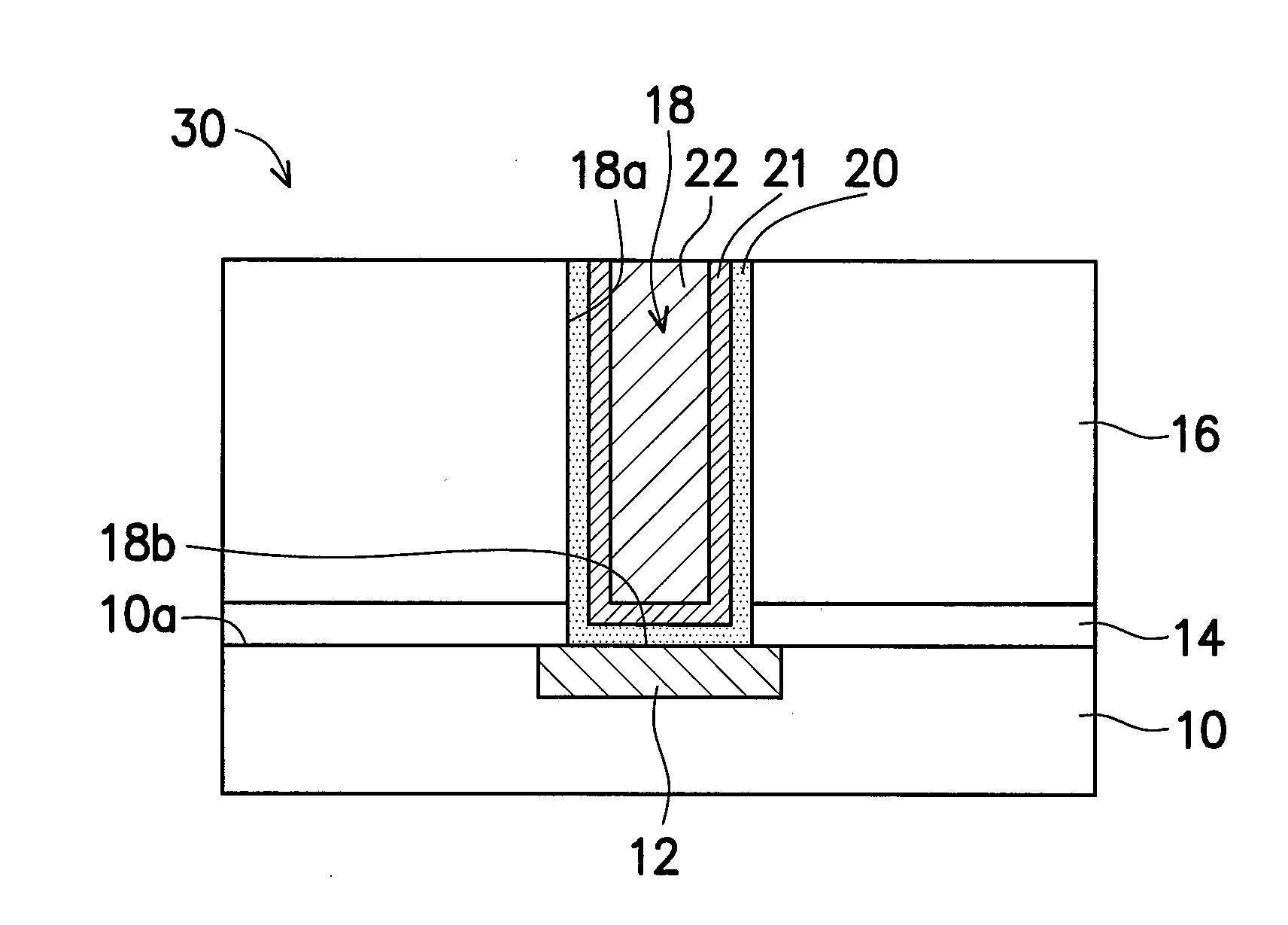
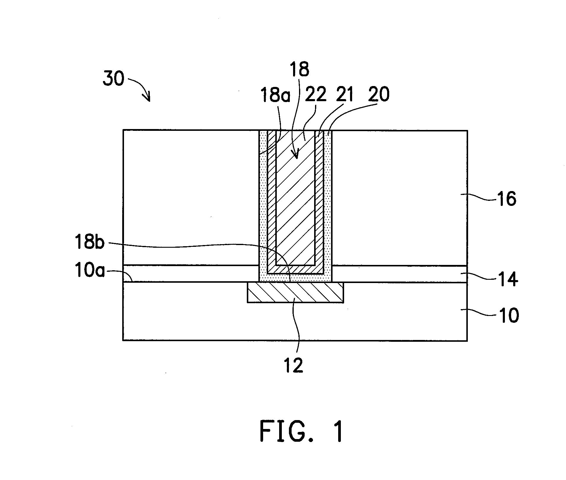
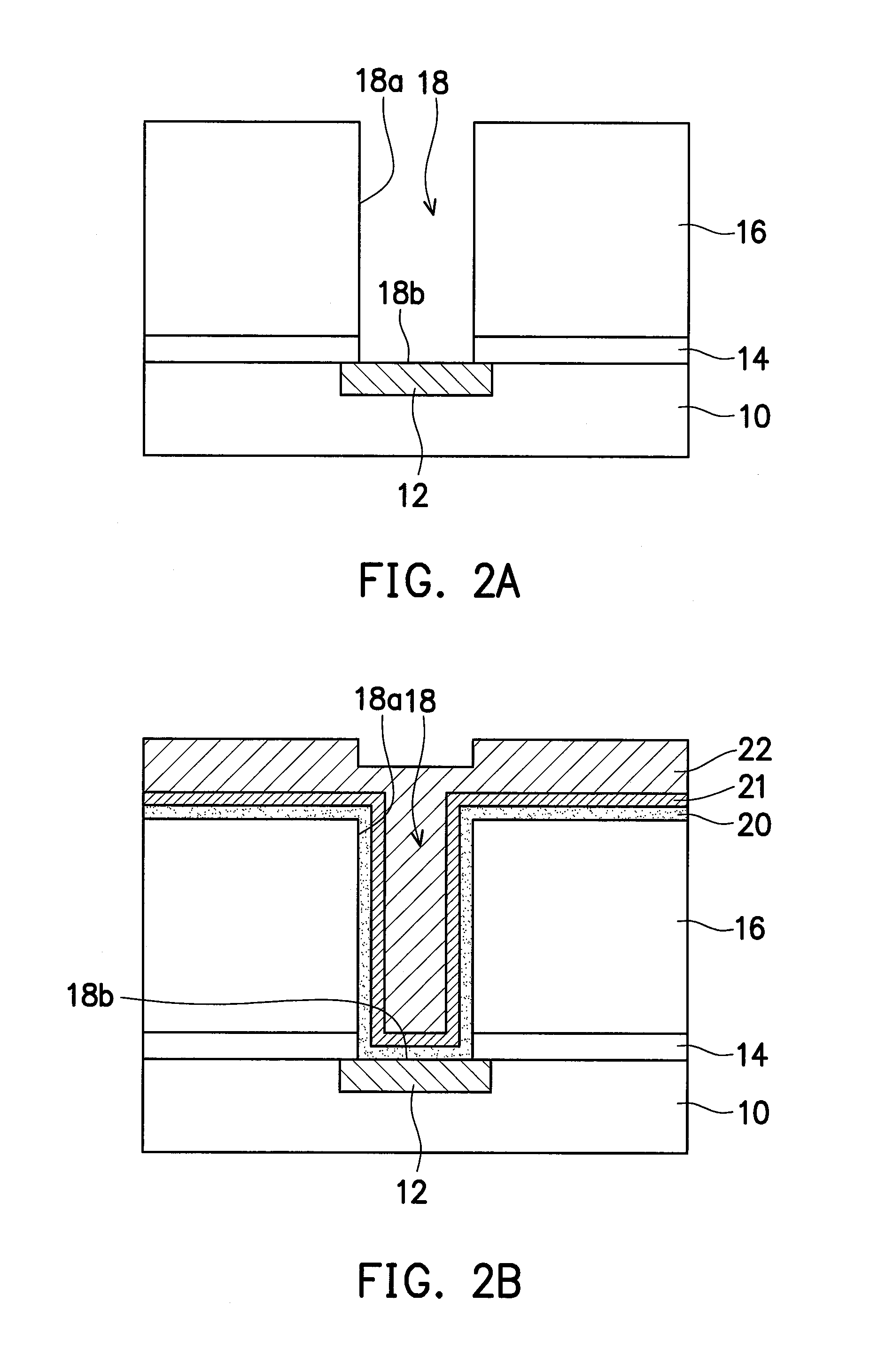
[0036]FIG. 1 schematically illustrates a cross-sectional view of a single metal damascene structure according to an embodiment of the present invention.

[0037]The single metal damascene structure 30 of the present invention includes a dielectric layer 16, a barrier layer 20, a seed layer 21 and a metal filling layer 22. The dielectric layer 16 has an opening 18 therein, and the opening 18 exposes the conductive region 12. The dielectric layer 16 includes a dielectric material, such as silicon oxide or a low-dielectric-constant (low-k) material with a dielectric constant less than 4. The opening 18 can be a hole extending in a single direction. The single direction can be a direction substantially perp...


PUM

PropertyMeasurementUnit
dielectric constantaaaaaaaaaa
conductiveaaaaaaaaaa
resistanceaaaaaaaaaa

Abstract

A single metal damascene structure including an insulating layer, a metal filling layer and a barrier layer is provided. The insulating layer has an opening therein, and the metal filling layer is positioned in the opening. The barrier layer is located between the filling metal layer and the insulating layer. The material of the barrier layer includes an alloy, and the ally includes a copper element and at least one another metal.

Description

BACKGROUND OF THE INVENTION[0001]1. Field of Invention[0002]The present invention relates to a single metal damascene structure and a method of forming the same.[0003]2. Description of Related Art[0004]A contact process is included between the front-end-of-line and back-end-of line process stages in the semiconductor device manufacture, so as to form contacts electrically connecting the device on the substrate and the metal lines.[0005]In the contact process, an interlayer dielectric layer is formed on the substrate having the device formed thereon, a contact opening is thereafter formed in the dielectric layer through photolithography and etching processes, and a tungsten plug is then formed in the contact opening.[0006]With minimization of the device, the resistance of the tungsten plug is increased as the dimension thereof is reduced, and the front-end performance degradation occurs. When the copper plug is used to replace the tungsten plug, the contact resistance can be reduced ...

Claims


Application Information

Patent Timeline
Patent Type & Authority Applications(United States)
IPC IPC(8): H01L23/522H01L21/768
CPCH01L21/76843H01L21/76856H01L21/76871H01L23/485H01L23/53238H01L23/53266H01L2924/0002H01L2924/00
Inventor CHEN, CHIEN-FU
Owner UNITED MICROELECTRONICS CORP
Why Eureka
Try Eureka