Semiconductor device and method for driving the same

Active Publication Date: 2013-11-14
SEMICON ENERGY LAB CO LTD
View PDF5 Cites 15 Cited by
  • Summary
  • Abstract
  • Description
  • Claims
  • Application Information

AI Technical Summary

Benefits of technology

[0020]In the above-described embodiment, with the use of the transistor with small off-state current, electric discharge at the time of stopping supply of the power supply voltage can be prevented, and quick charge of a capacitor can be performed at the time of restarting suppl

Problems solved by technology

As described above, in the structure in which supply of power supply voltage to the integrator circuit is stopped and restarted,

Method used


Image

  • Semiconductor device and method for driving the same
  • Semiconductor device and method for driving the same
  • Semiconductor device and method for driving the same

Examples


embodiment 1

[0036]In this embodiment, a circuit configuration of an integrator circuit that is a semiconductor device and a driving method of the integrator circuit will be described.

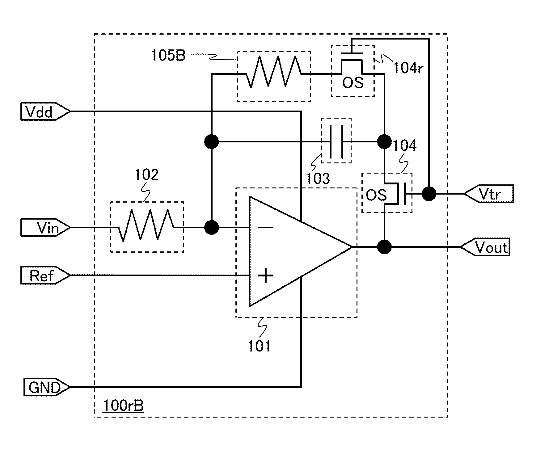
[0037]An integrator circuit 100 illustrated in FIG. 1 includes a differential amplifier circuit 101, a resistor 102, a capacitor 103, and a transistor 104.

[0038]The differential amplifier circuit 101 is supplied with power supply voltage by a high power supply potential Vdd and a ground potential GND. Note that the ground potential may be a low power supply potential Vss. The potential of a wiring which is supplied with the high power supply potential Vdd is changed from the high power supply potential Vdd to the ground potential GND, whereby supply of the power supply voltage to the differential amplifier circuit 101 is stopped. Further, the potential of the wiring supplied with the high power supply potential Vdd is set from the ground potential GND to the high power supply potential Vdd, whereby supply of the po...

embodiment 2

[0104]In this embodiment, a modified example of the integrator circuit 100 described above in Embodiment 1 will be described.

[0105]An integrator circuit 100rp illustrated in FIG. 6 includes the differential amplifier circuit 101, the resistor 102, the capacitor 103, and a transistor 104rp.

[0106]The structure in FIG. 6 is obtained by placing the transistor 104rp on the one electrode side of the capacitor 103 instead of placing the transistor 104 on the other electrode side of the capacitor 103 in FIG. 1 of Embodiment 1. When the transistor 104rp is placed on the inverting input terminal side of the differential amplifier circuit 101 instead of being placed on the output terminal side of the differential amplifier circuit 101, parasitic capacitance due to the transistor on the output terminal side can be reduced.

[0107]An integrator circuit 100rA illustrated in FIG. 10A includes the differential amplifier circuit 101, the resistor 102, the capacitor 103, the transistor 104, and a resi...

embodiment 3

[0112]In this embodiment, a modified example of the integrator circuit 100 described above in Embodiment 1 is described.

[0113]An integrator circuit 100bg illustrated in FIG. 7 includes the differential amplifier circuit 101, the resistor 102, the capacitor 103, and a transistor 104bg.

[0114]In the structure in FIG. 7, the transistor 104bg including a back gate is used instead of the transistor 104 illustrated in FIG. 1 of Embodiment 1 and a back gate voltage Vbg for controlling a threshold voltage is input to the back gate of the transistor 104bg.

[0115]The structure in which the threshold voltage of the transistor 104bg is controlled by controlling the potential of the back gate voltage Vbg enables the integrator circuit 100bg illustrated in FIG. 7 to more surely perform operation such as holding of electric charge in the capacitor 103.

[0116]An integrator circuit 100W illustrated in FIG. 11 includes the differential amplifier circuit 101, a differential amplifier circuit 101W, the ...


PUM


Abstract

A semiconductor device including an integrator circuit, in which electric discharge from a capacitor can be reduced to shorten time required for charging the capacitor in the case where supply of power supply voltage is stopped and restarted, and a method for driving the semiconductor device are provided. One embodiment has a structure in which a transistor with small off-state current is electrically connected in series to a capacitor in an integrator circuit. Further, in one embodiment of the present invention, a transistor with small off-state current is electrically connected in series to a capacitor in an integrator circuit; the transistor is on in a period during which power supply voltage is supplied; and the transistor is off in a period during which supply of the power supply voltage is stopped.

Description

BACKGROUND OF THE INVENTION[0001]1. Field of the Invention[0002]The present invention relates to a semiconductor device which functions as an integrator circuit and a method for driving the semiconductor device. In particular, the present invention relates to a semiconductor device in which electric charge accumulated in a capacitor of an integrator circuit can be held even when a power source is turned off and a method for driving the semiconductor device.[0003]In this specification, a semiconductor device refers to a device including a semiconductor element. Therefore, integrator circuits which are to be described in this specification are semiconductor devices.[0004]2. Description of the Related Art[0005]An integrator circuit including a differential amplifier circuit (also referred to as an operational amplifier) is known as a circuit which is used for a loop filter or the like in a phase locked loop circuit (PLL circuit).[0006]A basic circuit configuration of the integrator cir...

Claims


Application Information

Patent Timeline
IPC IPC(8): H03K17/00
CPCH03K17/002G06G7/186H01L21/77H01L27/00H03F3/45076H03F2203/45116H03F2203/45332
Inventor YAMAMOTO, ROHWATANABE, KAZUNORI
Owner SEMICON ENERGY LAB CO LTD
Why Eureka
Try Eureka