Substrate for liquid crystal display panel and liquid crystal display device

a liquid crystal display panel and substrate technology, applied in semiconductor devices, instruments, optics, etc., can solve problems such as current leakage, effectively suppress the occurrence of crosstalk and flicker, and reduce the resistance of auxiliary capacitance wiring lines.

Inactive Publication Date: 2013-11-14
SHARP KK
View PDF1 Cites 68 Cited by
  • Summary
  • Abstract
  • Description
  • Claims
  • Application Information

AI Technical Summary

Benefits of technology

[0025]According to a substrate for a liquid crystal display panel and a liquid crystal display device of the present invention, a light-shielding element provided for reducing OFF-leak current of the thin-film transistor is used to lower the resistance of an auxiliary capacitance wiring line, thereby making it possible to effectively suppress the occurrence of crosstalk and flicker without lowering the aperture ratio.

Problems solved by technology

Some thin-film transistors used in the active matrix method have a leakage of current when light is radiated onto the channel.

Method used


Image

  • Substrate for liquid crystal display panel and liquid crystal display device
  • Substrate for liquid crystal display panel and liquid crystal display device
  • Substrate for liquid crystal display panel and liquid crystal display device

Examples


embodiment 1

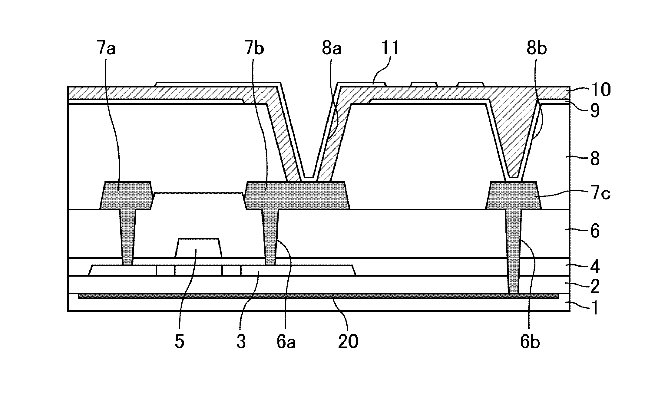
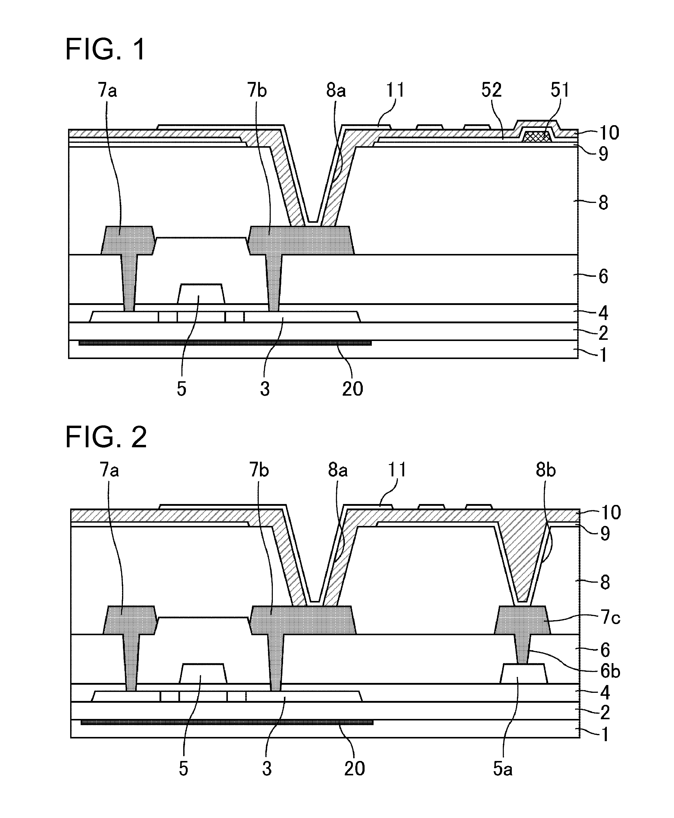
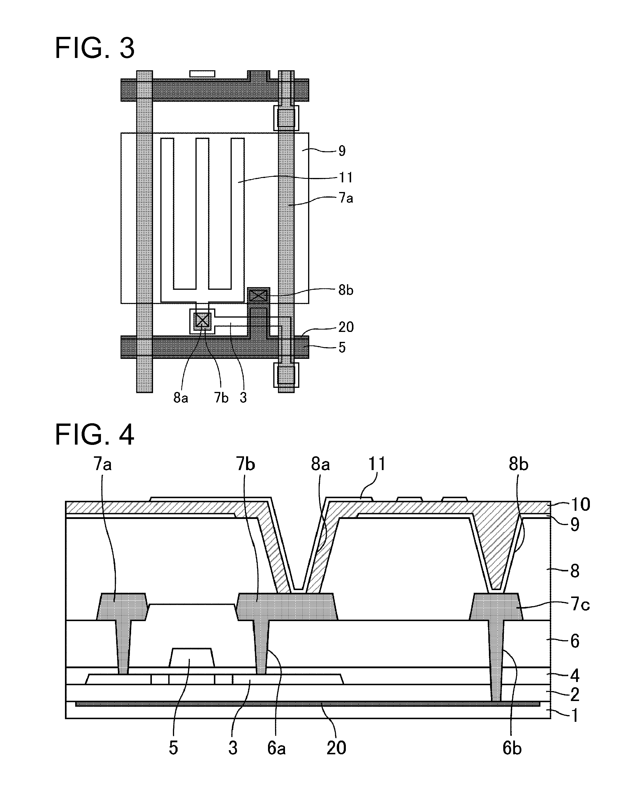
[0033]FIG. 1 is a cross-sectional schematic view showing a configuration of a substrate for a liquid crystal display panel of Comparison Example 1. FIG. 2 is a cross-sectional schematic view showing a configuration of a substrate for a liquid crystal display panel of Comparison Example 2. FIG. 3 is a plan schematic view showing a configuration of a substrate for a liquid crystal display panel of Embodiment 1. FIG. 4 is a cross-sectional schematic view showing a cross-section of the substrate for a liquid crystal display panel of FIG. 3. The substrate for a liquid crystal display panel of Comparison Examples 1 and 2 were not disclosed in the related art documents, but rather were created by the inventors of the present invention for contrast with the substrate for a liquid crystal display panel of the present embodiment.

[0034]The substrate for a liquid crystal display panel is built into a liquid crystal display device, with the liquid crystal display panel being manufactured by bond...

embodiment 2

[0070]A configuration of a substrate for a liquid crystal display panel of the present embodiment will be explained below with reference to FIGS. 6 and 7. FIG. 6 is a plan schematic view showing a configuration of a substrate for a liquid crystal display panel of Embodiment 2. FIG. 7 is a cross-sectional schematic view showing a cross-section of the substrate for a liquid crystal display panel of FIG. 6.

[0071]The substrate for a liquid crystal display panel of the present embodiment is used for an in-plane switching (IPS) mode liquid crystal display device, which is a type of transverse electric field mode. The common electrode 9 of Embodiment 1 covered the entire pixel, but a common electrode 9a of the present embodiment has a comb-teeth shape in a manner similar to a pixel electrode 11, and formed in the same layer as the pixel electrode 11. In the present embodiment, an auxiliary capacitance electrode 12 (a transparent electrode wiring line) is provided below an interelectrode in...


PUM

PropertyMeasurementUnit
thicknessaaaaaaaaaa
frequencyaaaaaaaaaa
thicknessaaaaaaaaaa

Abstract

The present invention provides a substrate for a liquid crystal display panel, the substrate being capable of effectively suppressing the occurrence of crosstalk and flicker without decreasing the aperture ratio. One aspect of the present invention is a substrate for a liquid crystal display panel, provided with: a light-shielding electroconductive member; a thin-film transistor arranged in a layer above the light-shielding electroconductive member; a transparent electrode wiring line arranged in a layer above the thin-film transistor, and a pixel electrode arranged in a layer above the transparent electrode wiring line. The light-shielding electroconductive member is a light-shielding element that covers the channel region of the thin-film transistor and is a wiring line connected to the transparent electrode wiring line, and the transparent electrode wiring line has a portion opposing the pixel electrode, with an insulating film disposed therebetween.

Description

TECHNICAL FIELD[0001]The present invention relates to a substrate for a liquid crystal display panel and a liquid crystal display device. More specifically, the present invention relates to a substrate for a liquid crystal display panel suitable for an active matrix method that uses thin-film transistors, and to a liquid crystal display device provided with the substrate for a liquid crystal display panel.BACKGROUND ART[0002]Liquid crystal display devices are display devices that use a liquid crystal composition for display. A representative display method therefor is a method that controls the light transmission amount by applying a voltage to liquid crystal sealed between a pair of substrates to change the orientation state of liquid crystal in accordance with the applied voltage.[0003]The passive matrix method and active matrix method are well known as driving methods for liquid crystal display devices. In typical active matrix liquid crystal display devices, gate bus lines and s...

Claims


Application Information

Patent Timeline
Patent Type & Authority Applications(United States)
IPC IPC(8): G02F1/1362H01L29/786
CPCG02F1/136209H01L29/78609G02F1/136213G02F1/136286G02F2201/124G02F2201/40H01L29/78633H01L29/78648H01L27/124G02F1/134363G02F1/1368G02F2202/16G02F2203/09G02F1/133397G02F1/134372
Inventor OKAJIMA, NAMIFUJIWARA, MASAHIRO
Owner SHARP KK
Why Eureka
Try Eureka