Capacitive Sensor Packaging

a sensor and capacitive technology, applied in the field of circuits and packaging for fingerprint sensors, can solve the problems of limiting the size and position of fingerprint recognition sensors, and limiting the design flexibility of fingerprint recognition sensors

Active Publication Date: 2013-11-21
APPLE INC
View PDF6 Cites 273 Cited by
  • Summary
  • Abstract
  • Description
  • Claims
  • Application Information

AI Technical Summary

Benefits of technology

[0012]In one embodiment, circuits may embody or employ techniques which use elements of the device to aid the fingerprint recognition sensor in fingerprint recognition. For some examples, circuits can be disposed using one or more device elements, with the one or more device elements assisting the fingerprint recognition sensor circuit by one or more of (1) coupling capacitive elements to a side of the device or near a button or other device element, (2) printing circuit elements to assist the fingerprint recognition sensor, or included in the fingerprint recognition sensor, on an underside of a button or other device element, (3) coupling fingerprint recognition sensor circuit elements to a button or other device element which improves coupling an electric field of the fingerprint recognition sensor, such as an anisotropic element including sapphire or another substance, and (4) using a transparent or translucent button or other device element to perform optical sensing or infrared sensing in addition to capacitive sensing, to assist or be included in the fingerprint recognition sensor circuit.

Problems solved by technology

This can have the effect of limiting the design flexibility for the fingerprint recognition sensor.
For example, the user's finger might have to be placed within a conductive ring, significantly limiting the size and position of the fingerprint recognition sensor.
This can also have the effect of limiting the design flexibility for the fingerprint recognition sensor.
Each of these examples, as well as other possible considerations, can cause difficulty for the fingerprint recognition sensor, and for the device incorporating the fingerprint recognition sensor (such as a computing device using fingerprint recognition for authentication).
The fingerprint recognition sensor might be limited in size, or position, or in whether it can be relatively easily incorporated with other elements of the device incorporating the fingerprint recognition sensor.
For a first example, this can have the effect that the fingerprint recognition sensor might not be easily incorporated into some types of devices (such as relatively small devices like smartphones and touchpads).
For a second example, this can have the effect that the fingerprint recognition sensor might be required to be relatively fragile or otherwise subject to unwanted design constraints.

Method used


Image

  • Capacitive Sensor Packaging
  • Capacitive Sensor Packaging
  • Capacitive Sensor Packaging

Examples


Embodiment Construction

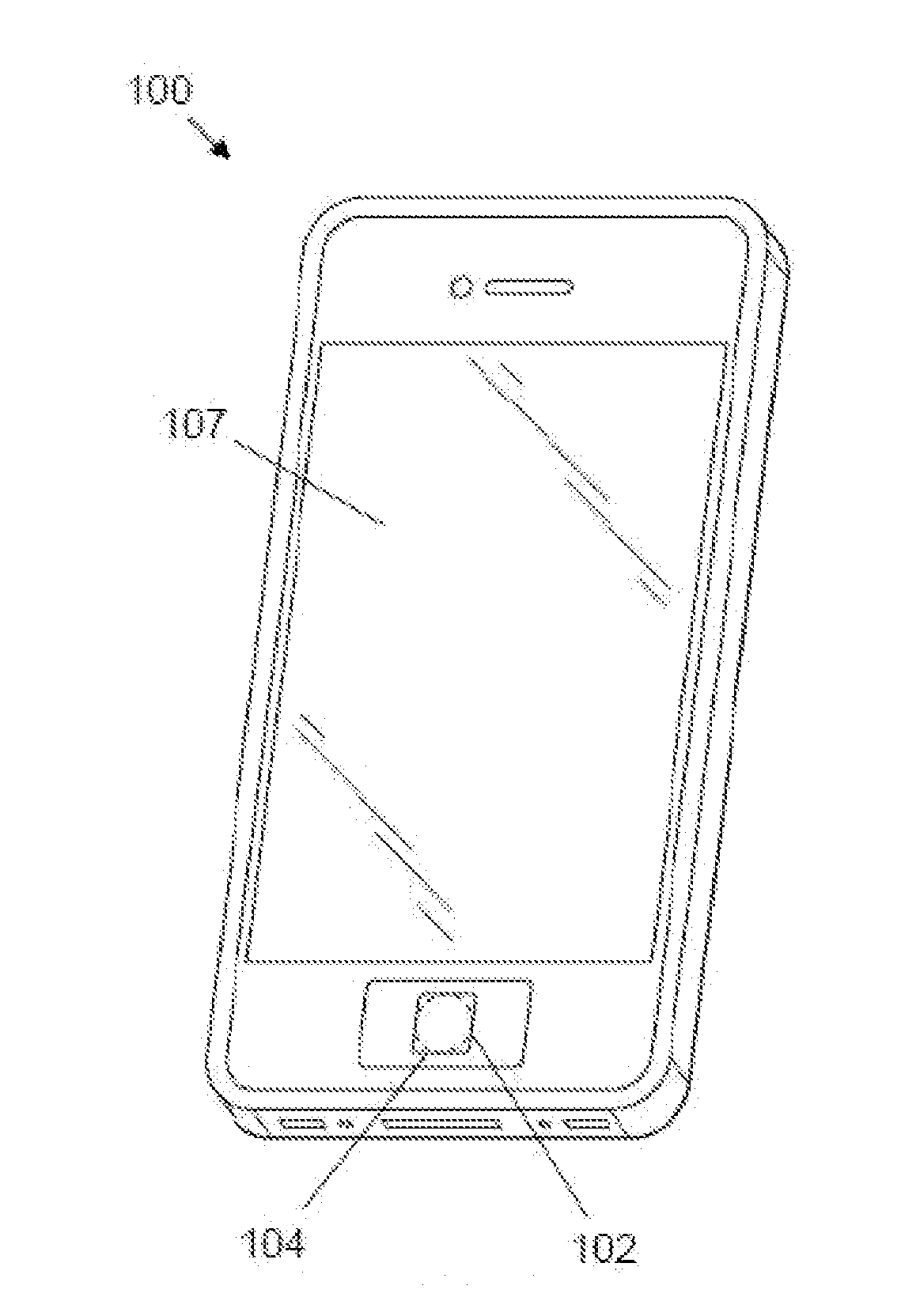
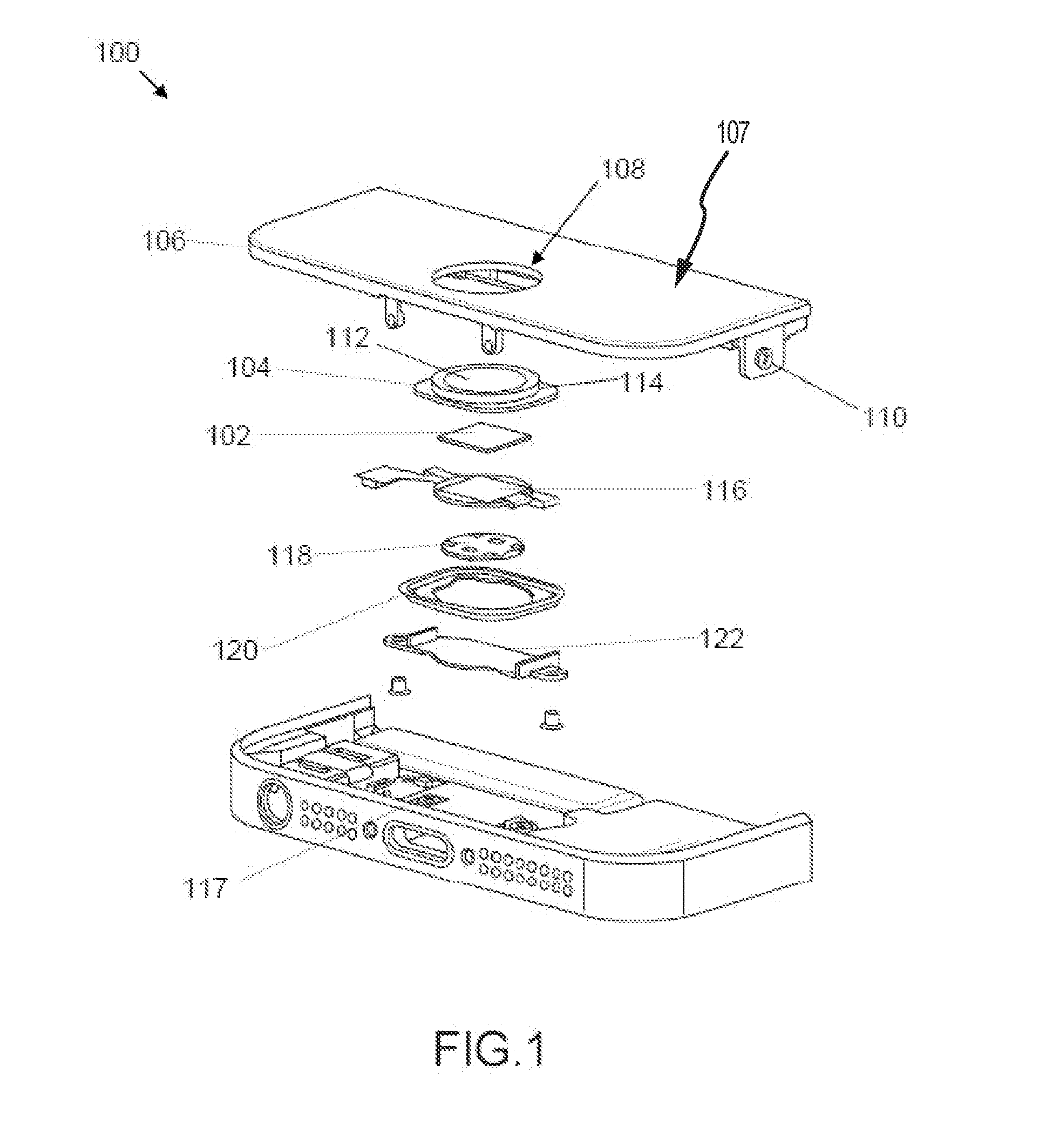
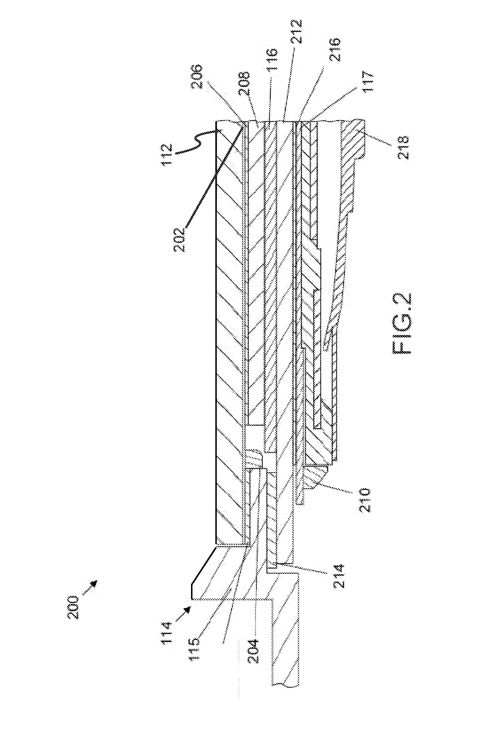
[0023]This disclosure is directed to fingerprint sensor systems for electronic devices, including, but not limited to, fingerprint image sensors for smartphones (or smart phones), tablet computers, media players, personal computers, and other portable electronics and mobile devices. In some designs, the fingerprint sensor is disposed beneath a control button or display element, so that fingerprint recognition and authentication can be performed while the device is being operated by a user.

[0024]The fingerprint sensor itself may utilize a grid of capacitive elements for capturing the fingerprint image, or an optical sensor or other suitable fingerprint imaging technology. A control circuit can also be provided, for example a control button or switch element responsive to touch or pressure, or a touchscreen control system responsive to proximity and (multiple) touch positioning. In some designs, the fingerprint sensor is utilized in combination with a control button or display element...


PUM


Abstract

An apparatus comprises a fingerprint sensor having a set of capacitive elements configured for capacitively coupling to a user fingerprint. The fingerprint sensor may be disposed under a control button or display element of an electronic device, for example one or more of a control button and a display component. A responsive element is responsive to proximity of the user fingerprint, for example one or both of a first circuit responsive to motion of the control button, and a second circuit responsive to a coupling between the fingerprint and a surface of the display element. The fingerprint sensor is disposed closer to the fingerprint than the responsive element. The control button or display component may include an anisotropic dielectric material, for example sapphire.

Description

CROSS-REFERENCE TO RELATED APPLICATIONS[0001]This application claims priority to U.S. Provisional Application No. 61 / 649,217, filed May 18, 2012, entitled “Capacitive Sensor Packaging,” and U.S. Provisional Application No. 61 / 666,607, filed Jun. 29, 2012, entitled “Capacitive Sensor Packaging,” the entirety of which is incorporated by reference herein.BACKGROUND[0002]Field of the Disclosure. This application generally relates to circuits and packaging for fingerprint sensors.[0003]Background of the Disclosure. Capacitive sensing of fingerprints provides for collection of fingerprint information in response to distinct measures of capacitance between, on the one hand, one or more capacitive plates in a fingerprint recognition sensor, and on the other hand, ridges and valleys of a user's finger (such as the epidermis of the user's finger, or possibly, subdermal layers of the user's finger).[0004]It sometimes occurs that measurements of capacitance involve introduction of electric char...

Claims


Application Information

Patent Timeline
Patent Type & Authority Applications(United States)
IPC IPC(8): G06F3/044
CPCG06F3/044G06V40/1329G06V40/1318G06V40/1306G06V40/1353G06V40/1365
Inventor POPE, BENJAMIN J.ARNOLD, SHAWNCORLETT, BARRY J.GILTON, TERRY L.HUSAINI, SYEDWEBSTER, STEVENMYERS, SCOTT A.HILL, MATTHEW D.LYON, BENJAMIN B.
Owner APPLE INC
Why Eureka
Try Eureka