Oxide thin film transistor, method for fabricating tft, display device having tft, and method for fabricating the same

a thin film transistor and oxide technology, applied in the field of thin film transistors, can solve the problems of large number of processes, failure to maintain initial performance, and limitation of a-si tft having mobility of 0.5 cm2/vs, and achieve the effect of enhancing element reliability

Active Publication Date: 2013-11-28
LG DISPLAY CO LTD
View PDF2 Cites 35 Cited by
  • Summary
  • Abstract
  • Description
  • Claims
  • Application Information

AI Technical Summary

Benefits of technology

[0029]An aspect of the present invention provides an oxide thin film transistor (TFT) capable of enhancing element reliability by preventing light supplied from the exterior or interior of an element from being made incident to an active layer, a method for fabricating the TFT, a display device having the TFT, and a method for fabricating the display device.

Problems solved by technology

However, as displays tend to have a large size and high picture quality, high device performance is required, and thus, it is determined that an existing a-Si TFT having mobility of 0.5 cm2 / Vs has reached a limitation.
Also, a-Si TFT has a problem of reliability in that as it continues to operate, device characteristics continue to be degraded to result in a failure of maintaining initial performance.
However, a fabrication of a poly-Si TFT requires a large number of processes in comparison to the a-Si TFT and investment in additional equipment should be made first.
Thus, p-Si TFT may be appropriately applied to make a display have high picture quality or applied to a product such as an OLED, or the like, but it is inferior to the existing a-Si TFT in terms of cost, so an application thereof is limited.
In particular, in the case of a p-Si TFT, due to a technical issue such as a limitation in fabrication equipment or a defect in uniformity, a fabrication process using a large substrate having a size of 1 m has not been realized so far, so the difficulty of the p-Si TFT in its application to a TV product is a factor making it difficult for high performance p-Si TFT to be easily settled down in the market.
However, in the case of the TFT employing oxide semiconductor according to the related art, when light irradiated, the element may be degraded.
Thus, when a negative bias is applied to a TFT having such an oxide semiconductor, a threshold voltage is rapidly shifted in a negative direction, degrading reliability.
Thus, when the related art TFT structure employing oxide semiconductor is applied as an element of a liquid crystal panel using a backlight and an OLED device employing compensation pixels, the element cannot be normally driven due to scattered-reflection of light generated from the organic light emitting layer.

Method used


Image

  • Oxide thin film transistor, method for fabricating tft, display device having tft, and method for fabricating the same
  • Oxide thin film transistor, method for fabricating tft, display device having tft, and method for fabricating the same
  • Oxide thin film transistor, method for fabricating tft, display device having tft, and method for fabricating the same

Examples


Embodiment Construction

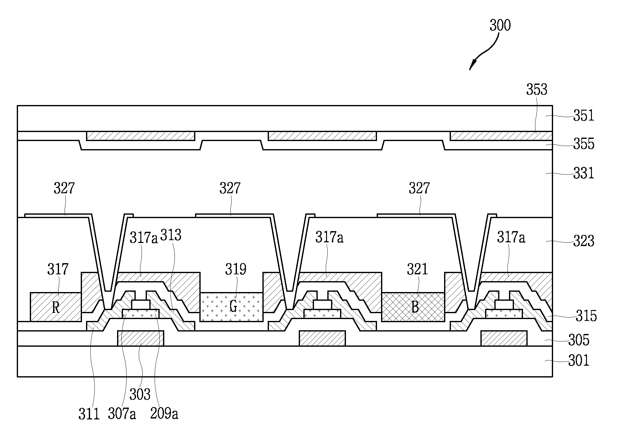
[0051]An oxide thin film transistor (TFT) structure according to embodiments of the present invention will be described in detail with reference to the accompanying drawings.

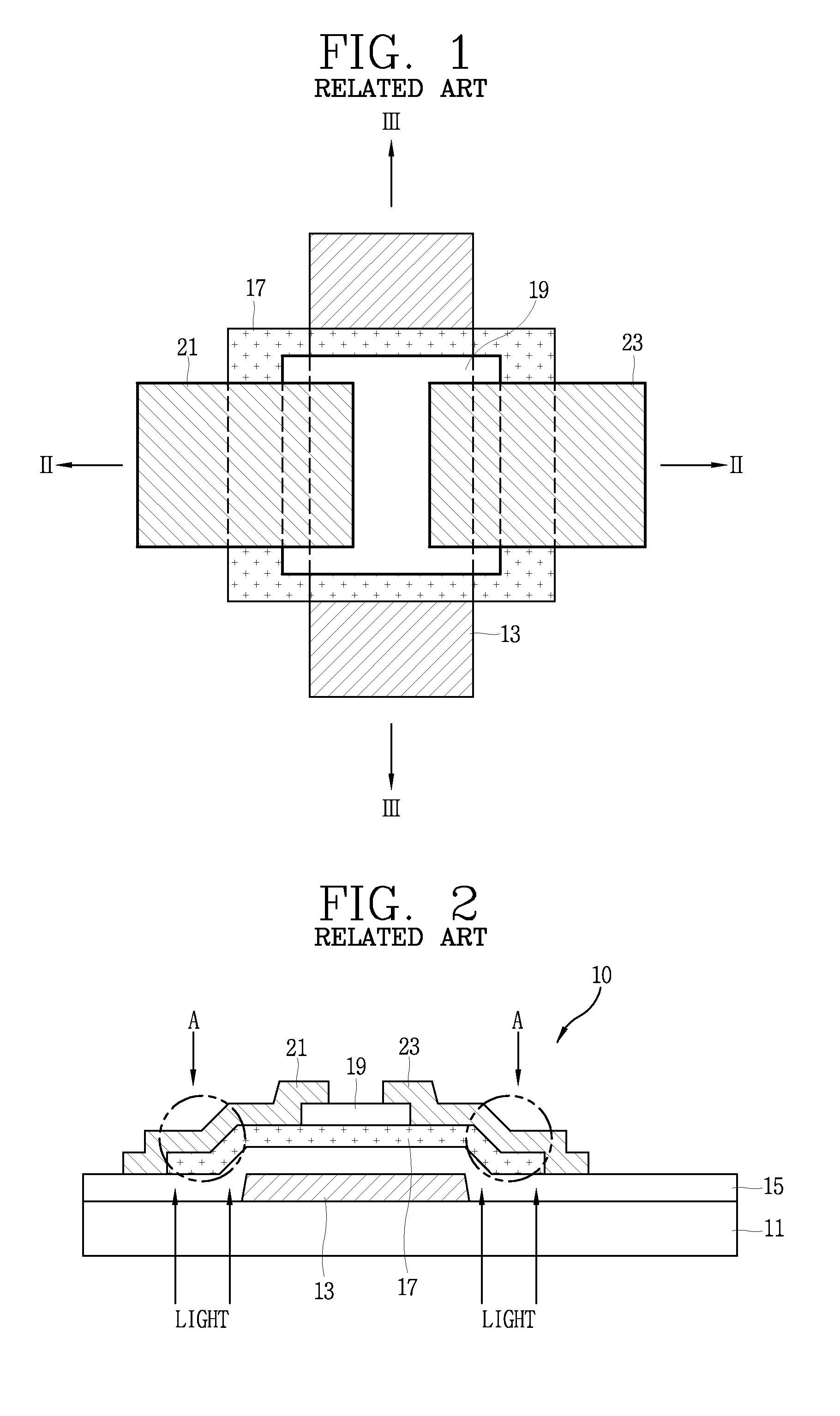
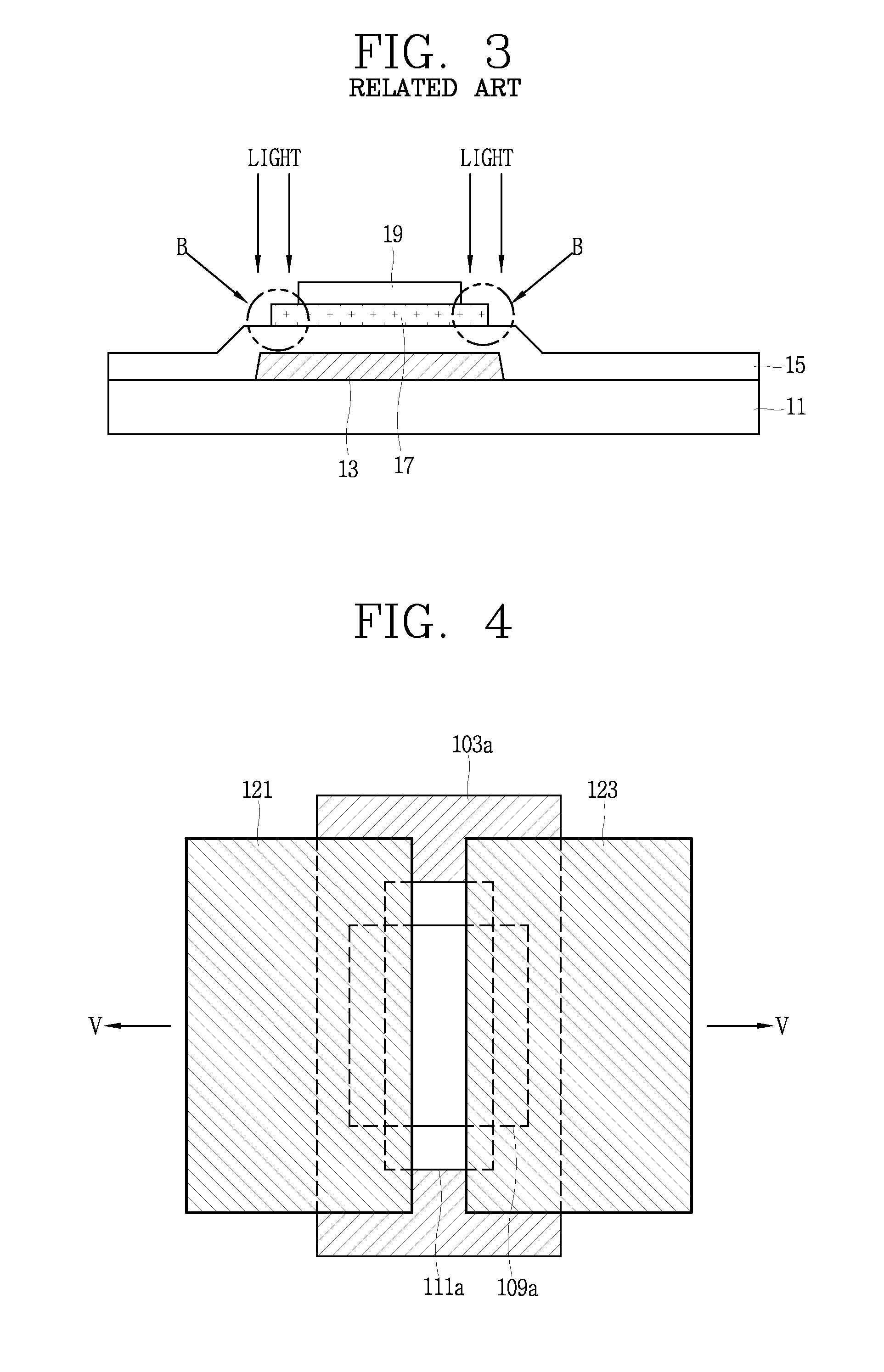
[0052]FIG. 4 is a plan view illustrating a structure of an oxide TFT according to an embodiment of the present invention.

[0053]FIG. 5 is a cross-sectional view taken along line V-V in FIG. 4, schematically illustrating an oxide thin film transistor (TFT) according to an embodiment of the present invention.

[0054]As illustrated in FIGS. 4 and 5, an oxide TFT 100 according to an embodiment of the present invention includes a gate electrode 103a formed on a substrate 101; a gate insulating layer 107 formed on the entire surface of the substrate 101 including the gate electrode 103a; an active layer pattern 109a formed on the gate insulating layer 107 above the gate electrode 103a and completely overlapping the gate electrode 103a; an etch stop layer pattern 111a formed on the active layer pattern 109a and the gate i...


PUM

PropertyMeasurementUnit
sizeaaaaaaaaaa
sizeaaaaaaaaaa
line widthaaaaaaaaaa

Abstract

There are provided an oxide TFT, a method for fabricating a TFT, an array substrate for a display device having a TFT, and a method for fabricating the display device. The oxide thin film transistor includes: a gate electrode formed on a substrate; a gate insulating layer formed on the entire surface of the substrate including the gate electrode; an active layer pattern formed on the gate insulating layer above the gate electrode and completely overlapping the gate electrode; an etch stop layer pattern formed on the active layer pattern and the gate insulating layer; and a source electrode and a drain electrode formed on the gate insulating layer including the etch stop layer pattern and the active layer pattern and spaced apart from one another, and overlapping both sides of the etch stop layer pattern and the underlying active layer pattern.

Description

[0001]The present disclosure relates to subject matter contained in priority Korean Application No. 10-2012-0055658, filed on May 24, 2012, which is herein expressly incorporated by reference in its entirety.1. FIELD OF THE INVENTION[0002]The present invention relates to a thin film transistor (TFT) and, more particularly, to an oxide TFT, a method for fabricating a TFT, a display device having a TFT, and a method for fabricating the display device.2. DESCRIPTION OF THE RELATED ART[0003]Television products are the major application targets in the remarkably growing flat panel display market. Currently, a liquid crystal display (LCD) is a mainstream as a TV panel, and research into an application of an organic light emitting display device to TVs has been actively ongoing.[0004]Current TV display techniques are focused on major items required in the market, and the requirements in the market include a large-scale TV or digital information display (DID), low cost, high picture quality...

Claims


Application Information

Patent Timeline
Patent Type & Authority Applications(United States)
IPC IPC(8): H01L29/786H01L29/66
CPCH01L29/78693H01L29/66969H01L29/7869H01L29/42384H01L29/78606H01L29/66742H10K59/1213
Inventor SEO, HYUNSIKKIM, MOONGOOKIM, BONGCHULLEE, JEONGHOONRYOO, CHANGIL
Owner LG DISPLAY CO LTD
Why Eureka
Try Eureka