Method for manufacturing an LCD device employing a reduced number of photomasks

a technology of lcd device and photomask, which is applied in the field of display devices, can solve the problems of reducing the yield of misalignment between photomasks, requiring a large amount of cost and time to conduct one photolithography process, and reducing the number of photomask alignments, so as to reduce the number of photomasks , the effect of suppressing the reduction of the yield caused by misalignment with another photomask

Inactive Publication Date: 2010-11-30
SEMICON ENERGY LAB CO LTD
View PDF26 Cites 14 Cited by
  • Summary
  • Abstract
  • Description
  • Claims
  • Application Information

AI Technical Summary

Benefits of technology

[0015]By reducing the number of photomasks compared to that in the conventional manufacturing method which uses five photomasks, the number of alignments of photomasks is reduced, and reduction in yield caused by misalignment with another photomask is suppressed.
[0016]Further, by reducing the number of photomasks, a part of photolithography process can be omitted; therefore, manufacturing cost can be reduced and throughput can be improved.
[0017]Furthermore, by omitting a part of photolithography process, contamination (e.g., particle) which may be generated in the process can be prevented. Thus, yield and reliability are improved.
[0018]An object of the present invention is to reduce the number of photomasks in a manufacturing process of a semiconductor device. That is, by manufacturing a semiconductor device using a process of the present invention, time and cost for the process can be reduced. Although a conventional amorphous silicon TFT is generally manufactured using five photomasks, it is possible to manufacture a TFT using three photomasks or four photomasks, and reduce time and cost for manufacturing the TFT by the present invention.
[0019]Further, reliability of elements can be improved by covering the TFT with an insulating film completely. When a surface of a channel portion is exposed, impurities from the substrate and ambient atmosphere, such as boron and phosphorus, enter the channel portion. These may serve as donors, so off leakage current of TFT is increased and an adverse effect that threshold voltage of TFT is changed is expected. However, by covering the TFT with an insulating film completely, that effect can be suppressed. A protective film performs a function of preventing the source electrode and the drain electrode from oxidizing when the TFT is a bottom gate type. On the other hand, the protective film performs a function of preventing the gate electrode from oxidizing when the TFT is a top gate type.
[0020]Furthermore, in the present invention, a pixel electrode is positioned below the protective insulating film and a gate insulating film and at a bottom surface of an opening region whereas a conventional pixel electrode is formed in the top layer of stacked layers. Therefore, the gate insulating film and the protective insulating film function as partitions, and interaction of field effects between neighboring pixel electrodes is decreased, thereby suppressing crosstalk. In addition, only the protective film is formed as an interlayer film between the pixel electrode and a signal line conventionally. However, in the present invention, a gate protective film is also provided, so parasitic capacitance between a signal line and a pixel electrode can be reduced.

Problems solved by technology

Since such multiple processes are needed, a great deal of cost and time is needed to conduct one photolithography process.
In particular, as the pattern which is formed using photomasks becomes more precise, a misalignment between photomasks brings larger effect on yield than ever.

Method used


Image

  • Method for manufacturing an LCD device employing a reduced number of photomasks
  • Method for manufacturing an LCD device employing a reduced number of photomasks
  • Method for manufacturing an LCD device employing a reduced number of photomasks

Examples


embodiment mode 1

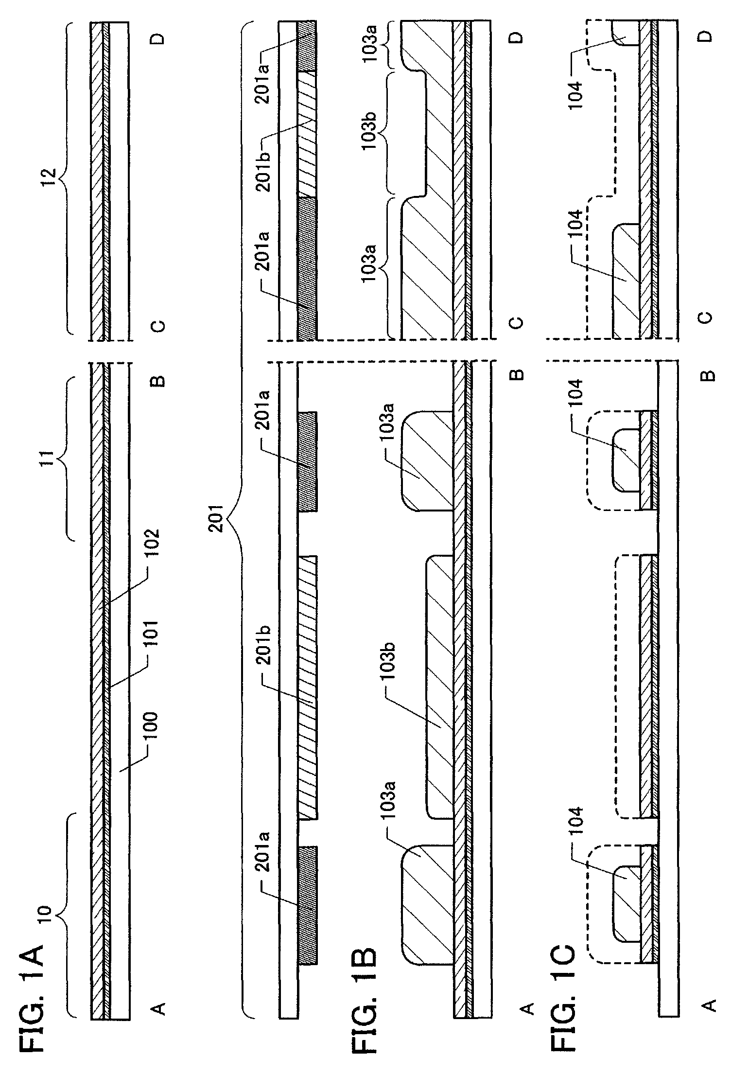
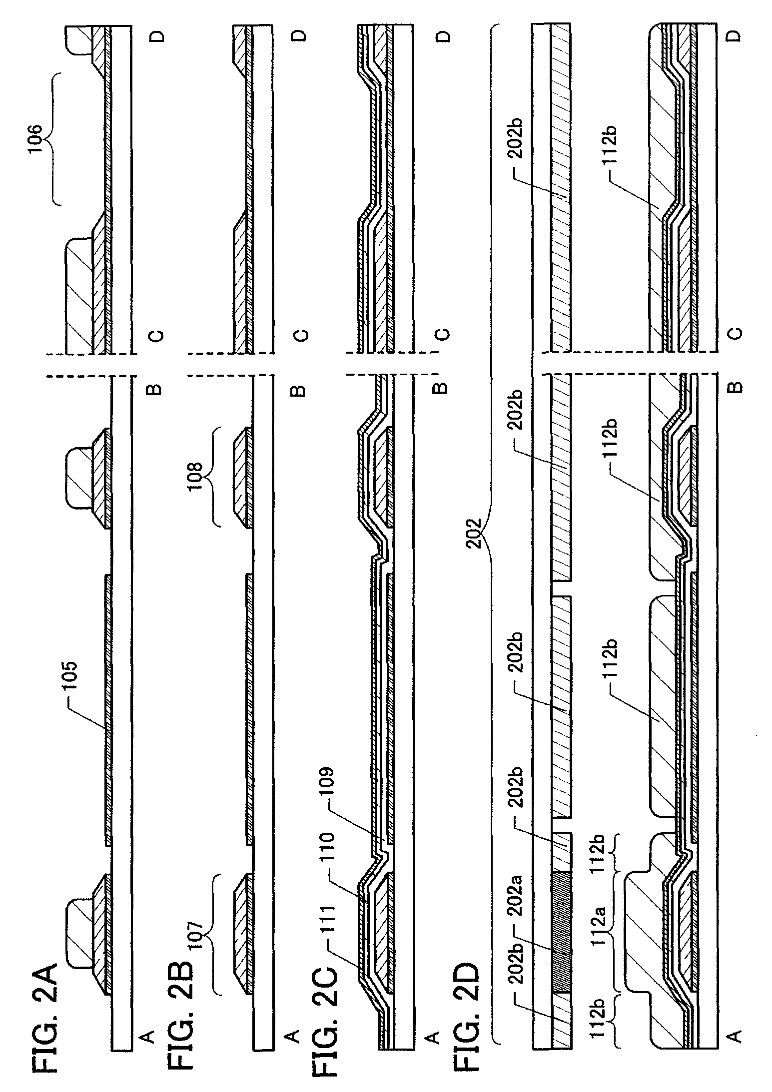
[0036]Description is made using a liquid crystal display device which is one mode of display modes. FIG. 11 is a plan view illustrating a TFT substrate of the liquid crystal display device according to Embodiment Mode 1. A region divided by scan lines 1101 and signal lines 1102 is one pixel, and a region in which a pixel electrode is formed in a pixel is referred to as a pixel region. A TFT 1103 which is a switching element of a pixel is in lower left portion in pixel. An on / off signal of TFT is input from the scan lines 1101 and a video signal is input from the signal lines 1102. The TFT 1103 is electrically connected to a pixel electrode 105 through a contact hole 113a, and the video signal input from the signal line is transmitted to the pixel electrode through the TFT when the TFT is in an on state. A storage capacitor 1104 is formed in upper right portion in pixel. The storage capacitor 1104 has a function that stores the video signal input into the pixel electrode 105 until su...

embodiment mode 2

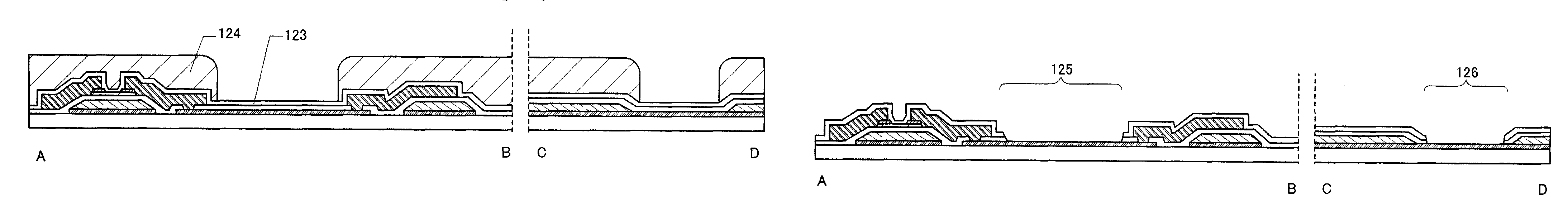
[0066]Then, in FIGS. 6A to 6C and 7A and 7B, a process using three photomasks of the present invention is described. In this process, the steps to the step for forming a source electrode and a drain electrode are similar to the process using four photomasks which is illustrated in FIGS. 1A to 1C, FIGS. 2A to 2D, FIGS. 3A to 3C, and FIGS. 4A to 4C of Embodiment Mode 1; therefore, the description thereof is omitted.

[0067]In FIG. 6A, the protective insulating film 123 formed of a silicon nitride film or the like is formed over the entire surface of the substrate by a CVD method. Then, a photoresist 601 is formed over a portion in which the first conductive layer and the second conductive layer are present by exposing process from the back surface of the substrate by backside light exposure. Here, since portions in which the transparent conductive film is formed of a single layer and which are not covered with electrodes formed of the second conductive layer transmit light, it is import...

embodiment mode 3

[0073]A process using three photomasks of a top gate type TFT using the present invention is described. FIG. 12 is a plan view illustrating a TFT substrate of a liquid crystal display device according to Embodiment Mode 3. A region divided by scan lines 1201 and signal lines 1202 is one pixel. A TFT 1203 which is a switching element of a pixel is in lower left portion in pixel. An on / off signal of TFT is input from the scan lines 1201 and a video signal is input from the signal lines 1202. The TFT is electrically connected to a pixel electrode 811, and the video signal input from the signal line is transmitted to the pixel electrode through the TFT when the TFT is in an on state. A storage capacitor 1204 is formed in upper right portion in pixel. The storage capacitor 1204 has a function that stores the video signal input into the pixel electrode 811 until subsequent signal is input. In FIG. 12, a portion shown by a dotted line A-B corresponds to cross-sectional views of FIGS. 8A to...


PUM


Abstract

A manufacturing method of the present invention includes a process using a first multi-tone mask, in which a first conductive layer in which a transparent conductive layer and a metal layer are stacked over a substrate, a gate electrode formed of a first conductive layer, and a pixel electrode formed of a single layer of the transparent conductive layer are formed, a process using a second multi-tone mask, in which a contact hole to the pixel electrode, and an island of an i-type semiconductor layer and an n+ type semiconductor layer are formed after a gate insulating film, the i-type semiconductor layer, and the n+ type semiconductor layer are formed, a process using a third photomask, in which a source electrode and a drain electrode are formed after a second conductive layer is formed, and a process using a fourth photomask, in which an opening region is formed after a protective film is deposited.

Description

BACKGROUND OF THE INVENTION[0001]1. Field of the Invention[0002]The present invention relates to a semiconductor device which has a circuit including a thin film transistor formed using a semiconductor film, and also relates to a manufacturing method thereof. Further, the present invention relates to a display device and a manufacturing method thereof.[0003]2. Description of the Related Art[0004]Display devices are widely spread as displays of televisions and personal computers, cellular phones, and the like, in many of which a liquid crystal display device which uses a thin film transistor including an amorphous silicon (hereinafter, referred to as an amorphous silicon TFT) as a switching element is used. The amorphous silicon TFT is conventionally formed over a glass substrate by a known photolithography process using five photomasks as disclosed in Patent Document 1.[0005]Five photomasks described here include a first photomask for forming a gate electrode, a second photomask for...

Claims


Application Information

Patent Timeline
Patent Type & Authority Patents(United States)
IPC IPC(8): H01L21/00G09F9/30H01L21/336H01L29/786
CPCH01L27/1288H01L27/1214H01L21/32139H01L21/31144H01L21/0273G02F2001/136231G02F2001/136236G02F2201/50G02F2001/13606G02F2001/13625G02F1/13606G02F1/136236G02F1/13625G02F1/136231
Inventor FUJIKAWA, SAISHIHOSOYA, KUNIOCHIBA, YOKO
Owner SEMICON ENERGY LAB CO LTD
Why Eureka
Try Eureka