
Spatial light modulator, spatial light modulator array, and exposure apparatus

a spatial light modulator and array technology, applied in the direction of instruments, static indicating devices, optical elements, etc., can solve the problems of reducing the reliability of an element, increasing the overall mass of the movable section, and posing a limitation on high-speed movement, so as to improve the durability of the exposure apparatus, improve the reliability of the element, and improve the effect of the utilization factor of ligh

Inactive Publication Date: 2007-01-16
FUJIFILM HLDG CORP +1
View PDF3 Cites 14 Cited by
  • Summary
  • Abstract
  • Description
  • Claims
  • Application Information

AI Technical Summary

Benefits of technology

This design achieves reliable, high-speed operation at low voltage, facilitates miniaturization, and improves light utilization and resolution by maintaining non-contact displacement and reducing the footprint of the drive structure.

Problems solved by technology

However, since the landing piece of the yoke comes into contact with the lower address electrode, there arises van der Waals force or adhesion of the landing piece to the address electrode by means of impurities or an organic-based gas in the environment, thereby resulting in a problem of a decrease in the reliability of an element.
As a result, the overall mass of the movable section is increased, thereby posing a limitation on high-speed movement.
As a result, the electrostatic attractive force acting on the pixel mirror and the address electrodes and the electrostatic attractive force acting on the yoke and the address electrodes become smaller, thus posing a limitation on the tendency toward lower voltage and higher-speed driving.
Further, since a single trap electrode operates only the edge, there arises an inconvenience of a reduction in a range of action of an electric field to be trapped.
Hence, the footprint of the comb drive structure becomes larger, thereby posing difficulty in attaining miniaturization and an increase in resolution and a problem of a low utilization factor of light.

Method used


Image

  • Spatial light modulator, spatial light modulator array, and exposure apparatus
  • Spatial light modulator, spatial light modulator array, and exposure apparatus
  • Spatial light modulator, spatial light modulator array, and exposure apparatus

Examples


first modification

[First Modification]

[0250]FIG. 27 is an enlarged view of the principal section of the first modification of the sixth embodiment, wherein the microlens array shown in FIG. 26 is provided with a prism.

[0251]In this modification, the microlens array 113 of the spatial light modulator array 500 provided in the light source / SLM unit 129 is provide with a prism 161 which is arranged so as to correspond to the microlenses 115. The light entered the mirror section 27 at this refraction angle is reflected in a direction different from the incident direction when the mirror section 27 is located at an OFF tilt position and reflected in a direction identical with the incident direction when the mirror section 27 is located at an ON tilt position.

[0252]Consequently, according to the first modification, when the mirror section 27 and the microlenses 115 are disposed so as to oppose each other, provision of the prism 161 enables reflection of incident light without retaining the mirror section 2...

second modification

[Second Modification]

[0253]FIG. 28 is an enlarged view of the principal section of a second modification in which the light entering the microlens array is tilted.

[0254]In this modification, a polarized beam splitter 163 has a polarized light separation surface 163a for reflecting the incident light originating from the light source at an angle other than the right angles. The angle α of the polarized light separation surface 163a is arbitrarily set in accordance with the positions of the microlenses 115 and the position of the spatial light modulator 100.

[0255]Accordingly, according to the second modification, the angle α of the polarized light separation surface 163a is set to 45° or more, the reflection angle of the polarized light separation surface 163a becomes an obtuse angle, thereby enabling a reduction in the thickness of the polarized beam splitter 163. Since the angle α of the polarized light separation surface 163a is set such that an incident light path and a reflected ...

third modification

[Third Modification]

[0256]FIG. 29 is a block diagram showing a third modification in which the microlens-array is disposed on the part of the beam splitter from which light exits.

[0257]In this modification, a third lens array plate 165 is provided on the part of the polarized beam splitter 141 from which exposure light exits. The third lens array plate 165 gathers a luminous flux that has been reflected from the mirror section 27 and passed through the polarized beam splitter 141.

[0258]Consequently, according to this modification, an object of exposure 121 can be directly exposed to modulated light, and an optical system close to contact exposure can be configured.


PUM


Abstract

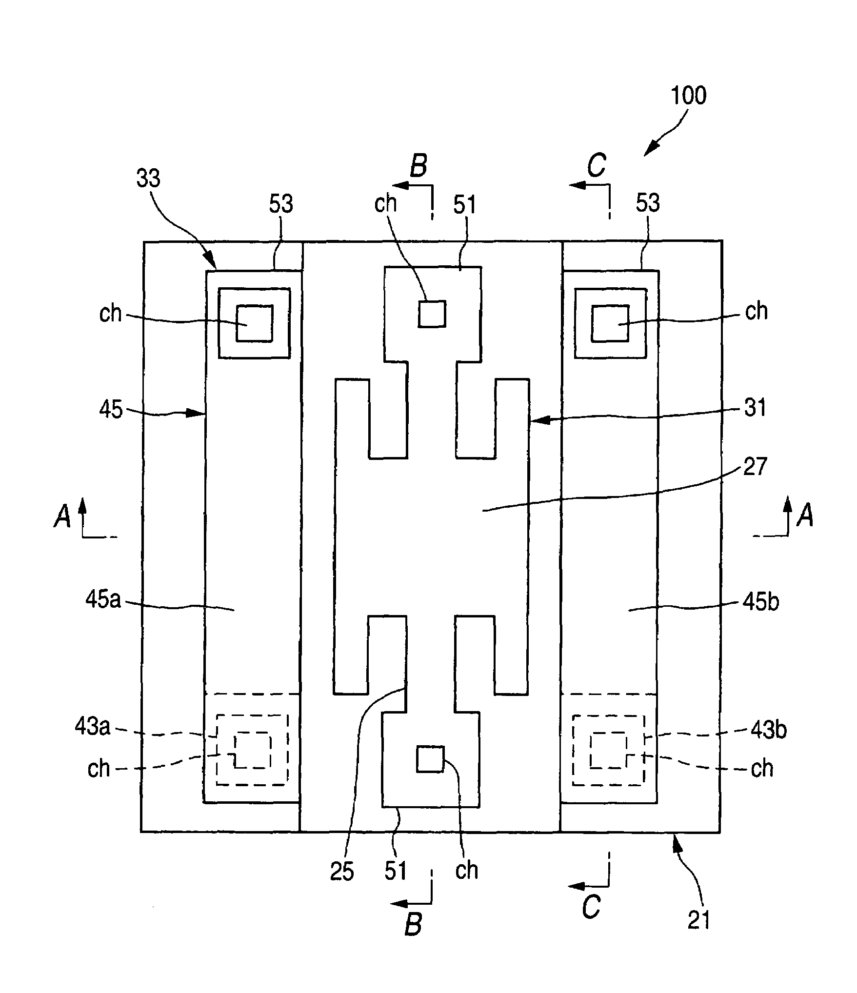
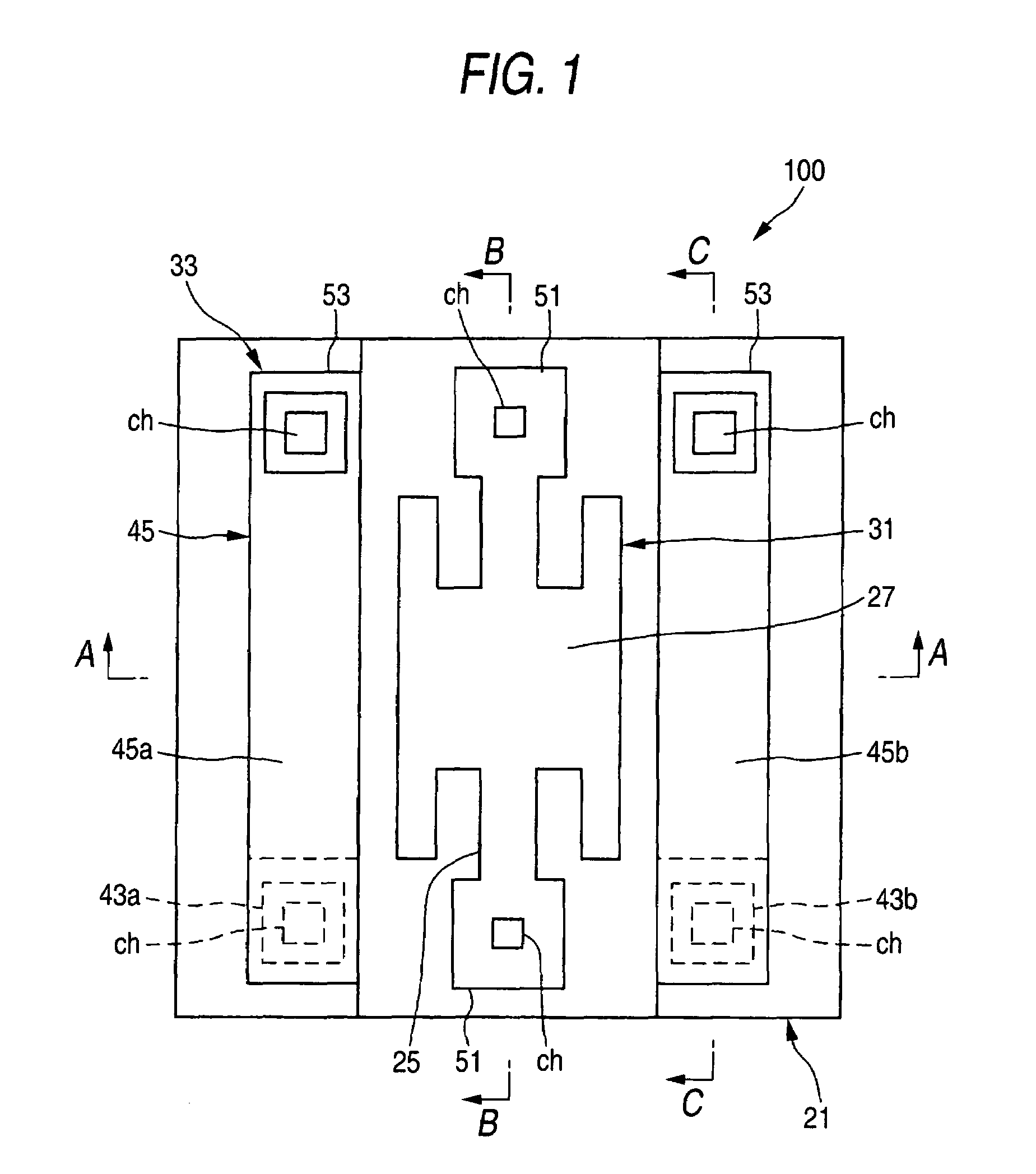
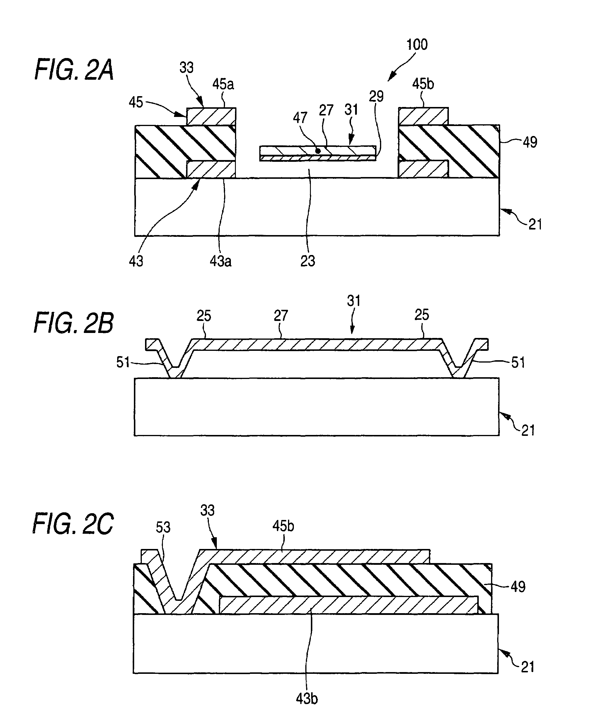
A spatial light modulator has a substrate; a movable member which is disposed so as to hang across the substrate in a displaceable manner and has a conductive section provided in at least a portion of the movable member; an optical function film which follows mechanical displacement of the movable member and is fixed to the same; and a drive fixed electrode which is disposed outside a range of mechanical displacement of the movable member and displaces and drives the movable member. Electrostatic attractive force is generated between the movable member and the driving fixed electrode by applying a drive voltage between the conductive section of the movable member and the driving fixed electrode, thereby displacing and driving the movable member, bringing the same into a stationary state in a non-contacting manner, and modulating light radiated on the optical function film.

Description

BACKGROUND OF THE INVENTION[0001]1. Field of the Invention[0002]The present invention relates to a spatial light modulator, a spatial light modulator array, and an exposure apparatus using them.[0003]2. Description of the Related Art[0004]A spatial light modulator (SLM) is a device for forming an optical image corresponding to an electrical or optical input. One type of SLM is a digital micromirror device (DMD) in which a micromirror is fabricated by means of a micro-mechanics technique and which attempts to deflect light by tilting the micromirror. The DMD is a monolithic single chip integrated circuit SLM and is constituted of a high-density array of movable micromirrors, each of which measures, e.g., 16 microns square. These mirrors are formed on an address circuit, thereby forming a pixel of the DMD array. When set at one of two positions the mirrors reflect incident light toward a projection lens, and when set at the other position deflect the incident light toward a light abso...

Claims


Application Information

Patent Timeline
Patent Type & Authority Patents(United States)
IPC IPC(8): G02B26/00G02B26/08G09G3/34B81B3/00B81B7/04
CPCG02B26/0841
Inventor KIMURA, KOICHISUMI, KATSUTO
Owner FUJIFILM HLDG CORP
Learn More