Display device

a display device and display technology, applied in the field of display devices, can solve the problems of display quality deterioration, difficulty in reversing the fluctuation potential of the auxiliary capacitance line to the original potential, etc., and achieve the effects of preventing the fluctuation of the pixel potential, reducing power consumption, and suppressing horizontal crosstalk

Inactive Publication Date: 2013-12-05
SHARP KK
View PDF2 Cites 8 Cited by
  • Summary
  • Abstract
  • Description
  • Claims
  • Application Information

AI Technical Summary

Benefits of technology

[0026]In any of the first to third aspects of the present invention, when the scanning signal line is in the selected state, the wiring to which the fixed potential is supplied, and the auxiliary capacitance line are electrically connected through the capacitive element in the smoothing part. Since this makes a potential fluctuation amount of the auxiliary capacitance line generated at the writing time of the data signal smaller than the conventional device, time till a potential of the auxiliary capacitance line returns to an original potential is made shorter than that in the conventional device. This prevents fluctuation of a pixel potential attributed to potential fluctuation of the auxiliary capacitance line from occurring. Moreover, since the potential of the auxiliary capacitance line is changed after the scanning signal line is switched from the selected state to the non-selected state, by which a bias voltage is applied to the pixel potential, a large voltage can be applied to a liquid crystal layer with a small data signal amplitude. Accordingly, horizontal crosstalk can be suppressed while reducing power consumption.
[0027]According to the fourth aspect of the present invention, the common electrode and the auxiliary capacitance line arranged along the scanning signal line in the se

Problems solved by technology

Particularly, in the conventional liquid crystal display device using the method of changing the potential of the corresponding auxiliary capacitance line after the selection period of each of the scanning signal lines has ended to thereby perform the reverse polarity driving, an impedance is raised by a switch or the like to switch the potential of the auxiliary capacitance line, which makes it difficult for the fluctuated potential of the auxiliary capacitance line to retur

Method used


Image

  • Display device
  • Display device
  • Display device

Examples


first embodiment

1. First Embodiment

1.1 Configuration of Liquid Crystal Display Device

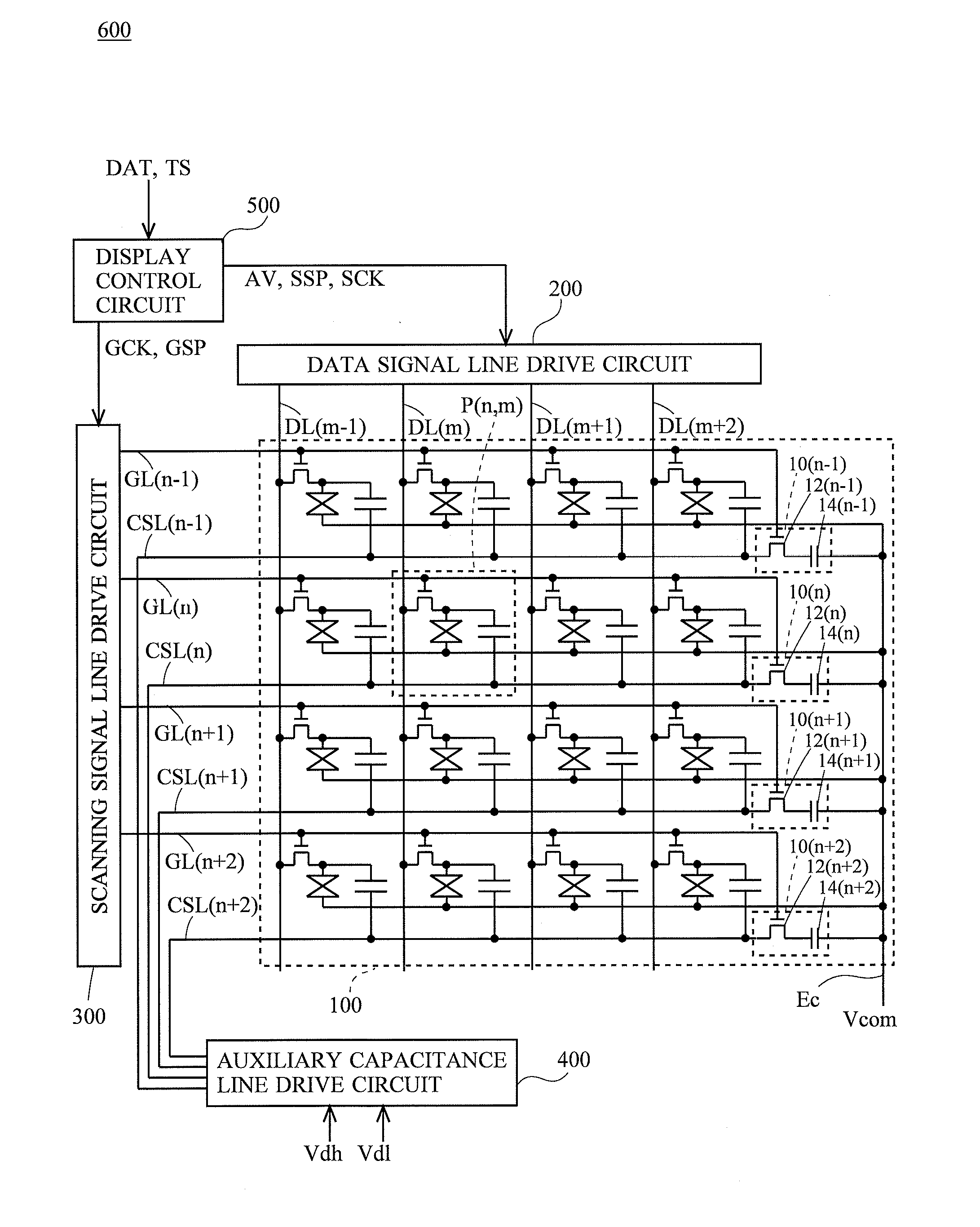
[0080]FIG. 1 is a circuit diagram showing an electric configuration of a liquid crystal display device 600 according to a first embodiment of the present invention. Of components of the present embodiment, the same components as those of the conventional liquid crystal display device 690 are denoted by the same reference characters, and descriptions thereof are omitted. As shown in FIG. 1, the liquid crystal display device 600 according to the present embodiment includes a display panel 100, a data signal line drive circuit 200, a scanning signal line drive circuit 300, an auxiliary capacitance line drive circuit 400, and a display control circuit 500. Any or all of the data signal line drive circuit 200, the scanning signal line drive circuit 300, the auxiliary capacitance line drive circuit 400 and the display control circuit 500 are mounted, for example, on a TFT substrate of the display panel 100 as an IC (Inte...

second embodiment

2. Second Embodiment

2.1 Configuration of Liquid Crystal Display Device

[0103]FIG. 9 is a circuit diagram showing an electric configuration of a liquid crystal display device 610 according to a second embodiment of the present invention. The liquid crystal display device 610 according to present embodiment includes a display panel 110 in place of the display panel 100 included in the liquid crystal display device 600 according to the first embodiment. Of components of the present embodiment, the same components as those of the first embodiment are denoted by the same reference characters, and descriptions thereof are omitted.

2.2 Configuration of Display Panel

[0104]In the display panel 110 in the present embodiment, unlike the display panel 100 in the first embodiment, smoothing parts 10 are provided on an input end side of auxiliary capacitance lines CSL (in FIG. 9, on the left side in the display panel 110). A position of each of the smoothing parts 10 is not limited to the input end...

third embodiment

3. Third Embodiment

3.1 Configuration of Liquid Crystal Display Device

[0111]FIG. 11 is a circuit diagram showing an electric configuration of a liquid crystal display device 620 according to a third embodiment of the present invention. The liquid crystal display device 620 according to present embodiment includes a display panel 120 in place of the display panel 100 included in the liquid crystal display device 600 according to the first embodiment. Of components of the present embodiment, the same components as those of the first embodiment are denoted by the same reference characters, and descriptions thereof are omitted.

3.2 Configuration of Display Panel

[0112]In the display panel 120 in the present embodiment, unlike the display panel 100 in the first embodiment, an auxiliary capacitance line CSL arranged along a corresponding scanning signal line GL, and an auxiliary capacitance line CSL arranged along a precedent scanning signal line GL of the scanning signal line GL in a scanni...


PUM


Abstract

A display panel of a liquid crystal display device includes smoothing parts provided on an output end side of auxiliary capacitance lines. Through the smoothing parts, the auxiliary capacitance lines arranged along scanning signal lines and a common electrode are connected to each other. The smoothing parts each have a correction TFT and a capacitor. A source electrode of the correction TFT and each of the auxiliary capacitance lines are connected to each other, and a drain electrode and the common electrode are connected to each other through each of the capacitors. The correction TFT is controlled so as to enter a conductive state when the scanning signal line is in a selected state, and enter a shut state when the scanning signal line is in a non-selected state.

Description

RELATED APPLICATIONS[0001]The present application is a National Phase of International Application Number PCT / JP2012 / 053089, filed Feb. 10, 2012, and which is based upon and claims the benefit of priority from Japanese Patent Application No. 2011-032563, filed on Feb. 17, 2011.TECHNICAL FIELD[0002]The present invention relates to a display device, and particularly, to an active matrix-type display device using switching elements such as thin film transistors.BACKGROUND ART[0003]In recent years, an active matrix-type display device such as a liquid crystal display device and an organic EL display device has been widely prevalent. Particularly, a liquid crystal display device in which a switching element such as a thin film transistor (TFT) is provided in each pixel circuit has attracted attention, because a display image with less crosstalk can be obtained even if the number of pixels is increased.[0004]The active matrix-type liquid crystal display device has conventionally been requ...

Claims


Application Information

Patent Timeline
IPC IPC(8): G09G3/36
CPCG09G3/3655G09G3/3648G09G2300/0876G09G2320/0209G09G2330/021
Inventor KUWABARA, NOBUHIRO
Owner SHARP KK
Why Eureka
Try Eureka