Nonvolatile semiconductor memory device of variable resistive type

a semiconductor memory and resistive type technology, applied in the direction of information storage, static storage, digital storage, etc., can solve the problems of difficult to control the period, current starts to flow, and is difficult to ensur

Active Publication Date: 2013-12-12
ELPIDA MEMORY INC
View PDF5 Cites 24 Cited by
  • Summary
  • Abstract
  • Description
  • Claims
  • Application Information

AI Technical Summary

Benefits of technology

[0012]In one embodiment, there is provided a device that includes: a memory including a variable resistive memory cell including first and second terminals, a variable resistive memory element coupled between the first and second terminals, and a select transistor coupled between the second terminal and a first voltage line; and a capacitor circuit configured to be connected to the first terminal of the variable resistive memory cell when the select transistor is selected to be conductive between the second terminal and the first voltage line, the first terminal of the variable resistive memory cell being increased in voltage by the capacitor circuit to change a resistivity of the variable resistive memory element from a first level to a second level that is smaller than the first level.

Problems solved by technology

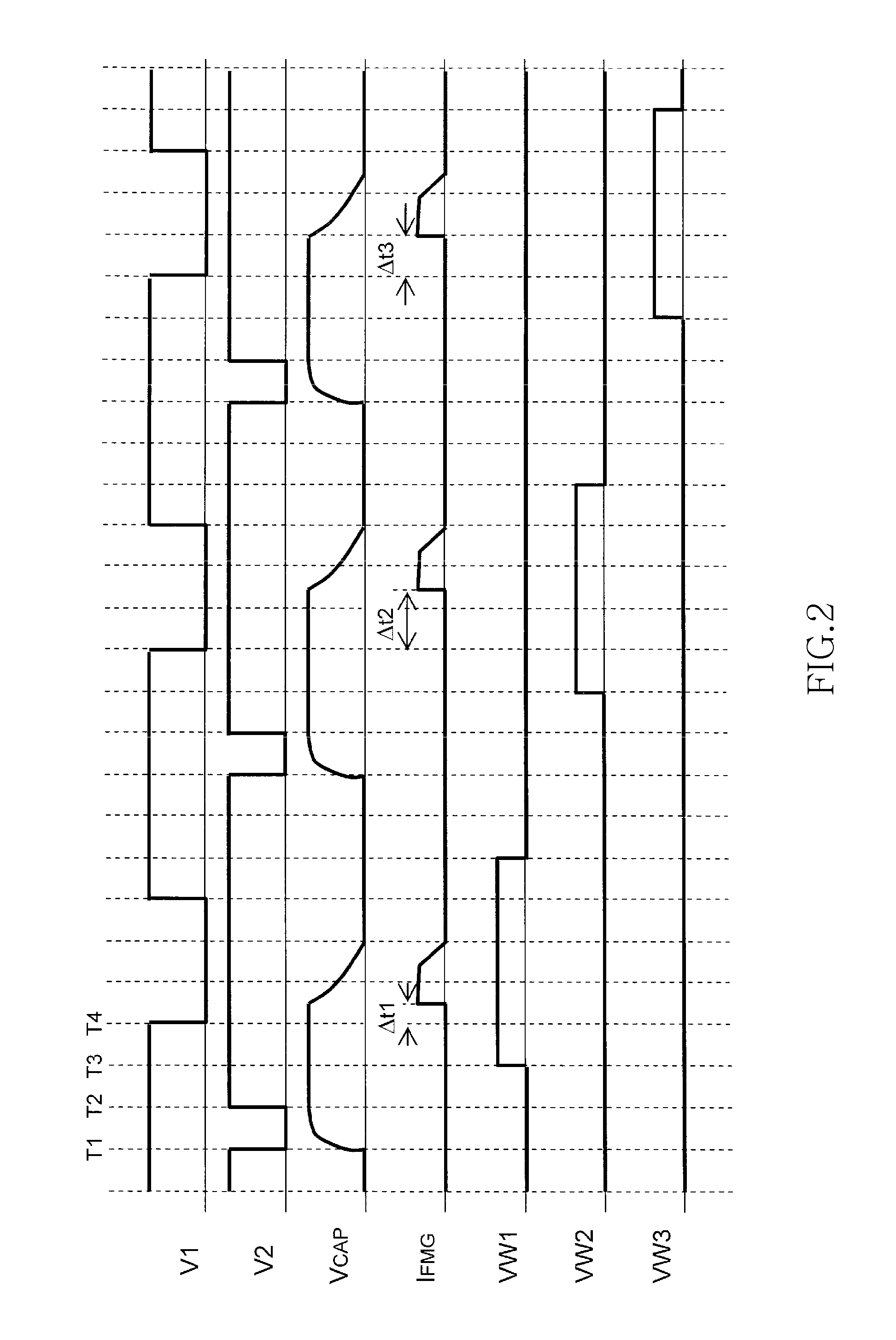
However, in principle, it is difficult to control the period from when a voltage is applied until when the breakdown starts. FIG. 10 shows changes of current over time which flows at a time when a forming voltage pulse is applied at two variable resistive elements where hafnium oxide (HfOx), which functions as a variable resistor, is held between a Ta electrode and a TiN electrode.
However, as the resistance rapidly drops due to the breakdown, the current starts to flow.
However, given the nature of the breakdown, it is difficult to ensure that the breakdown start time of one element is exactly the same as that of the other element.
As a result, there is concern that a difference would occur between the elements in terms of resistance switching characteristics.

Method used


Image

  • Nonvolatile semiconductor memory device of variable resistive type
  • Nonvolatile semiconductor memory device of variable resistive type
  • Nonvolatile semiconductor memory device of variable resistive type

Examples


first embodiment

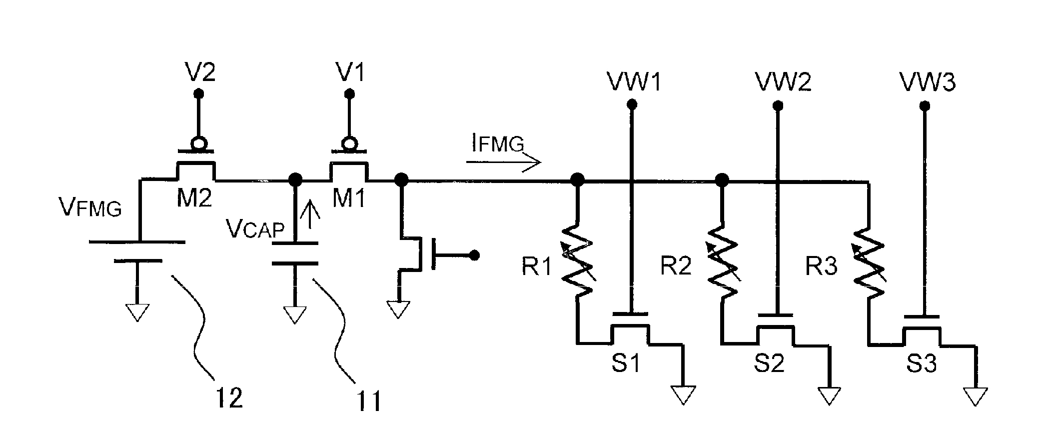
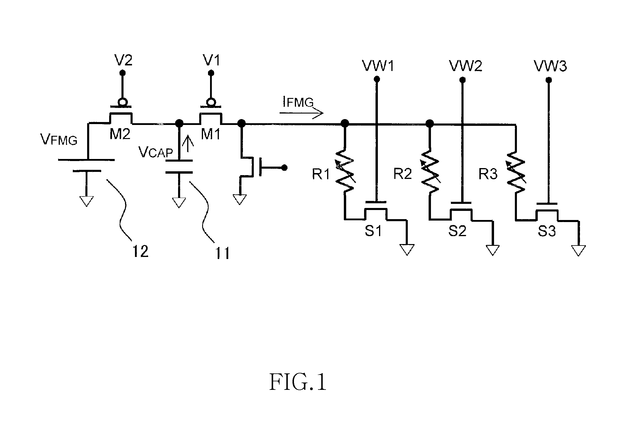
[0028]FIG. 1 shows an exemplary circuit diagram of a nonvolatile semiconductor memory device according to a first embodiment of the present invention.

[0029]In the nonvolatile semiconductor memory device according to the first embodiment of the present invention shown in FIG. 1, a plurality of variable resistive elements R1 to R3 each are connected in series to corresponding select transistors S1 to S3, thereby forming a memory cell. Voltages VW1 to VW3 are applied to the gates of the select transistors to select memory cells. The voltages and currents necessary for forming of the variable resistive elements R1 to R3 are supplied from a capacitor 11. One end of the capacitor 11 is connected to the memory cells via a PMOS switch M1, as well as to a power source 12 via a PMOS switch M2. The other end of the capacitor 11 is connected to a reference potential (e.g. GND). In the example shown in FIG. 1, PMOS transistors are used as switches M1 and M2. However, NMOS transistors may be used...

second embodiment

[0064]What is described in the above first embodiment is an example in which, during the forming process, the capacitor circuit 30 is used, and the forming voltage and current are supplied via the charged capacitor. Meanwhile, the transition (set operation) of the variable resistive elements from a high-resistance state to a low-resistance state is considered to be the same physical phenomenon as the forming. At the time of the lowering-resistance operation, the capacitor circuit 30 can be used.

[0065]In this case, if the amount of electric charge required for the forming process is different from the amount of electric charge required for the set operation, a plurality of capacitors can be used, and it is possible to switch between capacitors used for the forming process and capacitors used for the set operation. Alternatively, it is also preferred that all the plurality of capacitors be used during the forming process, and that some of the capacitors be used during the set operatio...


PUM


Abstract

Disclosed herein is a device that includes: a memory including a variable resistive memory cell including first and second terminals, a variable resistive memory element coupled between the first and second terminals, and a select transistor coupled between the second terminal and a first voltage line; and a capacitor circuit configured to be connected to the first terminal of the variable resistive memory cell when the select transistor is selected to be conductive between the second terminal and the first voltage line, the first terminal of the variable resistive memory cell being increased in voltage by the capacitor circuit to change a resistivity of the variable resistive memory element from a first level to a second level that is smaller than the first level.

Description

BACKGROUND OF THE INVENTION[0001]1. Field of the Invention[0002]The present invention relates to a nonvolatile semiconductor memory device, and more particularly to a nonvolatile semiconductor memory device using a variable resistive element that can store information by changing in electric resistance caused by applying of electric stress.[0003]2. Description of Related Art[0004]In recent years, the capacity of a nonvolatile semiconductor memory device as represented by a flash memory becomes remarkably larger. At the product level, products with a capacity of over 10 gigabytes are available at low prices. The value of the products is rising especially as portable or mobile memories such as USB memories, and the device is increasingly likely to grab shares of the market dominated by magnetic optical discs and the like. The capacity of several gigabytes is enough to serve as the storage of portable music players. Compared with a hard disk-equipped portable music player that has been...

Claims


Application Information

Patent Timeline
Patent Type & Authority Applications(United States)
IPC IPC(8): G11C13/00
CPCG11C13/0069G11C2213/32G11C2213/34G11C2213/79
Inventor TAMAI, YUKIOJONO, YUSUKE
Owner ELPIDA MEMORY INC
Why Eureka
Try Eureka