
Manufacturing method of circuit pattern

Inactive Publication Date: 2013-12-19
LEADING TECH COMM
View PDF8 Cites 0 Cited by
  • Summary
  • Abstract
  • Description
  • Claims
  • Application Information

AI Technical Summary

Benefits of technology

The invention provides a method for making a circuit pattern on a three-dimensional or curved surface, improving the manufacturing quality and saving costs. The method can use a variety of substrate materials, including plastic, and avoids color casts or costly laser cracks.

Problems solved by technology

Therefore, the performance of the antenna may be affected.
The mentioned disadvantages related to the antenna or the circuit pattern made by the laser direct structuring process needs to be further improved.

Method used


Image

  • Manufacturing method of circuit pattern
  • Manufacturing method of circuit pattern
  • Manufacturing method of circuit pattern

Examples


Embodiment Construction

[0020]An embodiment of the instant disclosure provides a manufacturing method of the circuit pattern, which can form a three-dimensional (or a curved surface) antenna structure as well as the circuit pattern for other purpose on the substrate. The above-mentioned method in the embodiment of the instant disclosure take the antenna structure manufacturing as an example, but manufacture of the antenna structure is not used to restrict the scope of this invention. In the present embodiment, the above-mention substrate might be the casing of smart mobile phone, which usually utilizes the plastic or glass substrate. However the instant disclosure is not used to restrict the kind of the substrate. In order to provide the sufficient binding strength between the antenna structure and the substrate, the manufacturing method of the antenna structure on the shell is taken as the example in this embodiment.

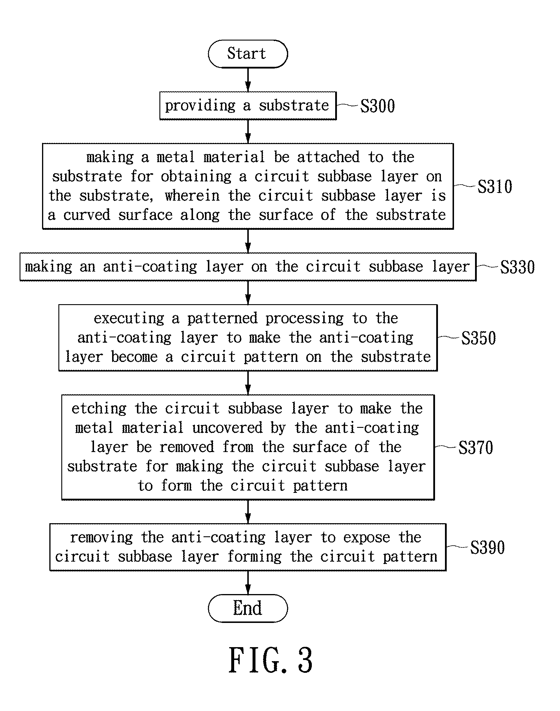
[0021]Referring to FIG. 3, FIG. 4A to FIG. 4F, FIG. 3 are the flow diagrams which describe...


PUM

PropertyMeasurementUnit
Percent by massaaaaaaaaaa
Diameteraaaaaaaaaa
Diameteraaaaaaaaaa

Abstract

This instant disclosure provides a manufacturing method of circuit pattern. The method comprising, providing a substrate; making a metal material be attached to the substrate for obtaining a circuit subbase layer on the substrate, wherein the circuit subbase layer is a curved surface along the surface of the substrate; making an anti-coating layer on the circuit subbase layer; executing a patterned processing to the anti-coating layer to make the anti-coating layer become an antenna pattern on the substrate; etching the circuit subbase layer to make the metal material uncovered by the anti-coating layer be removed from the surface of the substrate for making the circuit subbase layer to form the antenna pattern; removing the anti-coating layer to expose the circuit subbase layer forming the circuit pattern. Therefore, the manufacturing quality of the circuit pattern can be improved and the associated cost can be saved.

Description

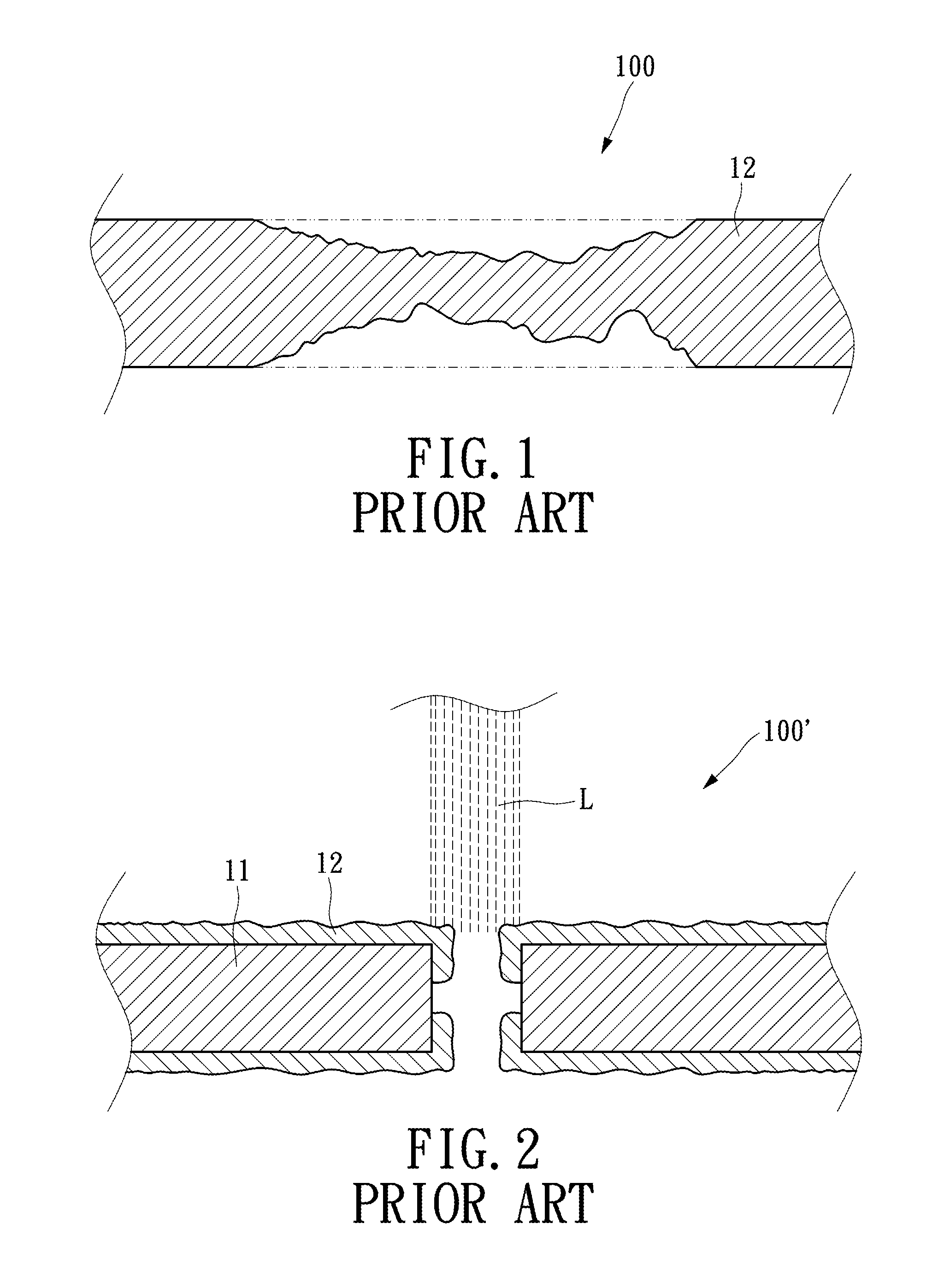
BACKGROUND[0001]1. Technical Field[0002]The invention relates to a circuit pattern, and in particular, to a manufacturing method of the circuit pattern.[0003]2. Description of Related Art[0004]FIG. 1 and FIG. 2 show cross-sectional diagrams of a traditional antenna structure 100, 100′. As shown in FIG. 1, a laser direct structuring (LDS) process is applied to a substrate 11 to make a laser activated layer 12. The substrate 11 may be a casing of a mobile device (e.g. smart phone). The laser activated layer 12 may not accord to a predetermined line width (defined by the dashed lines) because some areas are not activated by the laser, thus a jump-plated phenomenon may be occurred. Therefore, the performance of the antenna may be affected. As shown in FIG. 2, when a laser beam L is applied to a via hole of the substrate 11 for making the laser activated layer 12, some area of the via hole wall may not be totally activated due to the diameter of the via hole, the shape of the via hole or...

Claims


Application Information

Patent Timeline
IPC IPC(8): H05K3/06C25D5/02
CPCC23C18/1653C25D5/02C25D5/48H05K1/119H05K3/06H05K3/24H05K3/426
Inventor HUANG, HSING YA
Owner LEADING TECH COMM
Learn More