Integrated structure of compound semiconductor devices

Active Publication Date: 2013-12-19
WIN SEMICON
View PDF8 Cites 17 Cited by
  • Summary
  • Abstract
  • Description
  • Claims
  • Application Information

AI Technical Summary

Benefits of technology

[0004]The main object of the present invention is to provide an integrated structure of compound semiconductor devices, which includes an optimized HBT and an optimized varactor. The monolithically integrated structure is formed by inserting an n-type graded doping layer, an etching-stop layer, and a p-type doped layer below an HBT. The inserted layers together with the sub-collector layer of the HBT can be used to form a varactor, in which the doping concentration of the n-type graded doping layer is gradually increasing or decreasing from the p-t

Problems solved by technology

However, such a concentration gradient in the collector layer is detrimental for a

Method used


Image

  • Integrated structure of compound semiconductor devices
  • Integrated structure of compound semiconductor devices
  • Integrated structure of compound semiconductor devices

Examples


Example

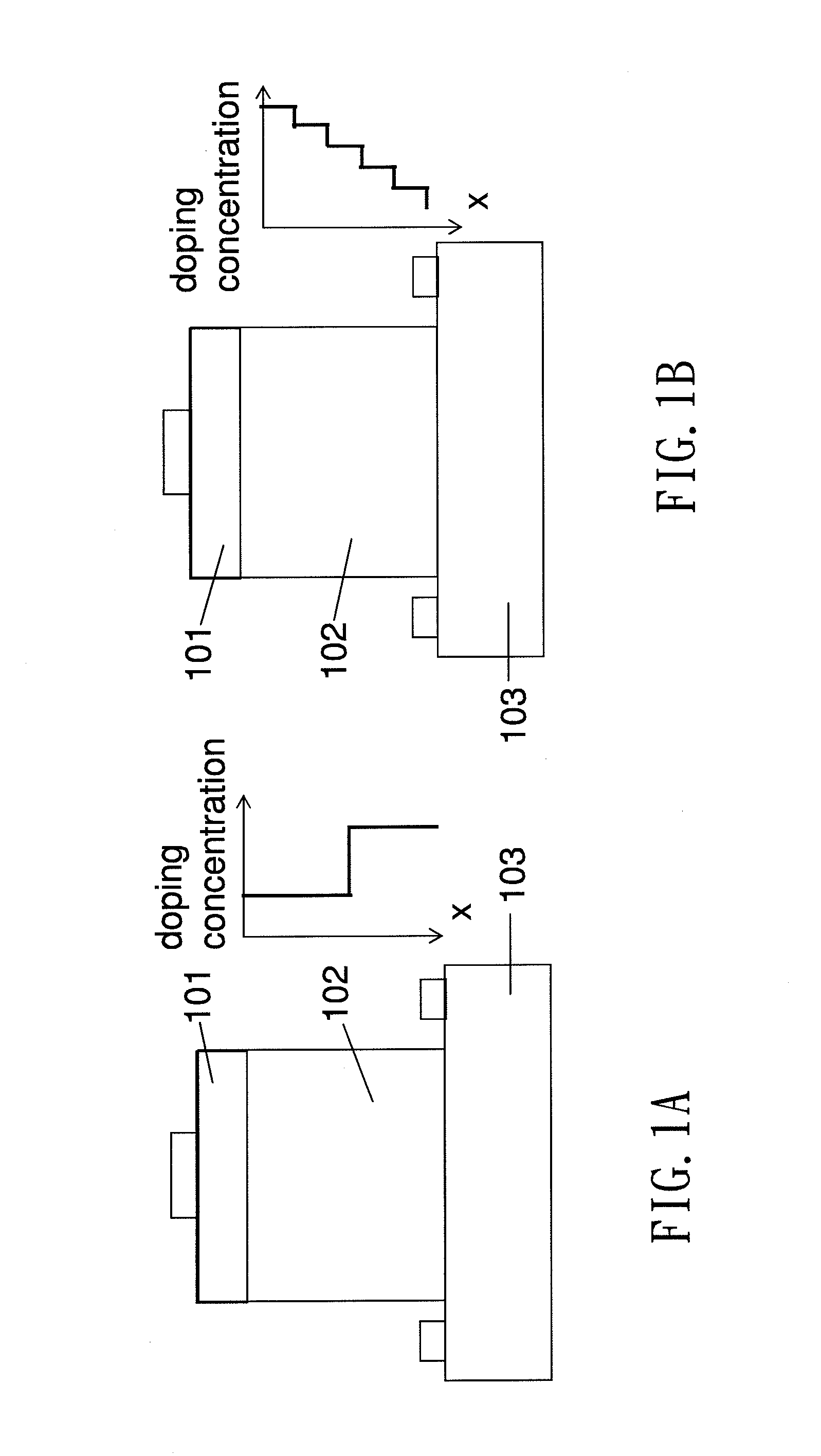
[0021]The integrated structure of compound semiconductor devices including an optimized BBT and an optimized varactor provided by the present invention is shown schematically in FIG. 2. The structure comprises a substrate 201, a first epitaxial layer 202, an etching-stop layer 203, a second epitaxial layer 204, a sub-collector layer 206, a collector layer 207, a base layer 208, and an emitter layer 209. The first epitaxial layer is a p-type doped layer.

[0022]In the structure stated above, the substrate 201 is made of a semi-insulating semiconductor material such as GaAs or InP. The first epitaxial layer 202 is a p-type doped layer formed on the substrate 201. The first epitaxial layer 202 is made preferably of GaAs. The thickness of the first epitaxial layer can be selected to be between 10 nm and 1000 nm, preferably between 10 nm and 100 nm. The doping concentration of the first epitaxial layer can be selected to be between 1×1015 cm−3 and 1×1022 cm−3, preferably between 1×1018 cm−...


PUM


Abstract

An integrated structure of compound semiconductor devices is disclosed. The integrated structure comprises from bottom to top a substrate, a first epitaxial layer, an etching-stop layer, a second epitaxial layer, a sub-collector layer, a collector layer, a base layer, and an emitter layer, in which the first epitaxial layer is a p-type doped layer, the second epitaxial layer is an n-type graded doping layer with a gradually increased or decreased doping concentration, and the sub-collector layer is an n-type doped layer. The integrated structure can be used to form an HBT, a varactor, or an MESFET.

Description

FIELD OF THE INVENTION[0001]The present invention relates to an integrated structure of compound semiconductor devices, and in particular, to a structure that can integrate a heterojunction bipolar transistor (HBT), a varactor, and a metal semiconductor field effect transistor (MESFET) on the same wafer for applications in voltage-controlled oscillators (VCO) and power amplifiers (PA).BACKGROUND OF THE INVENTION[0002]A voltage-controlled oscillator (VCO) device consists of two components: an HBT and a varactor. A varactor is an electronic device whose capacitance can be varied by changing the applied voltage. They are applied mainly in various tuning circuits. In conventional compound semiconductor manufacturing processes, the base-collector junction of an HBT is usually utilized as a varactor. FIG. 1A is a schematic showing the cross-sectional view of a conventional varactor, consisting of a p-type doped layer 101, a first n-type doped layer 102, and a second n-type doped layer 103...

Claims


Application Information

Patent Timeline
IPC IPC(8): H01L29/205
CPCH01L29/205H01L27/0605H01L29/20H01L29/36H01L29/7371H01L29/812H01L29/93
Inventor LIN, CHENG-KUOLI, SZU-JUSYU, RONG-HAOTSAI, SHU-HSIAO
Owner WIN SEMICON
Why Eureka
Try Eureka