Method and Apparatus for Electron Pattern Imaging

a technology of electron pattern and electron pattern, applied in the direction of material analysis using wave/particle radiation, instruments, nuclear engineering, etc., can solve the problems of diffraction characteristics of samples, insufficient beam current of most sems, and various deficiencies in current arrangement, so as to achieve the effect of safe operation of image intensifier

Inactive Publication Date: 2013-12-26
EDAX
View PDF1 Cites 2 Cited by
  • Summary
  • Abstract
  • Description
  • Claims
  • Application Information

AI Technical Summary

Benefits of technology

[0013]An object of the present invention is to amplify light in an EBSD pattern collection system using an image inte

Problems solved by technology

However, this current arrangement suffers from various deficiencies as discussed hereinafter.
Under low voltage and low current conditions, most SEMs do not provide sufficient beam current for optimal illumination of the phosphor screen.
Diffraction characteristics of the sample also create limitations in the current arrangement.
These conditions diffuse and/or weake

Method used


Image

  • Method and Apparatus for Electron Pattern Imaging
  • Method and Apparatus for Electron Pattern Imaging
  • Method and Apparatus for Electron Pattern Imaging

Examples


Embodiment Construction

[0025]For purposes of the description hereinafter, the terms “upper”, “lower”, “right”, “left”, “vertical”, “horizontal”, “top”, “bottom”, “lateral”, “longitudinal”, and derivatives thereof shall relate to the invention as it is oriented in the drawing figures. However, it is to be understood that the invention may assume various alternative variations, except where expressly specified to the contrary. It is also to be understood that the specific devices illustrated in the attached drawings, and described in the following specification, are simply exemplary embodiments of the invention. Hence, specific dimensions and other physical characteristics related to the embodiments disclosed herein are not to be considered as limiting.

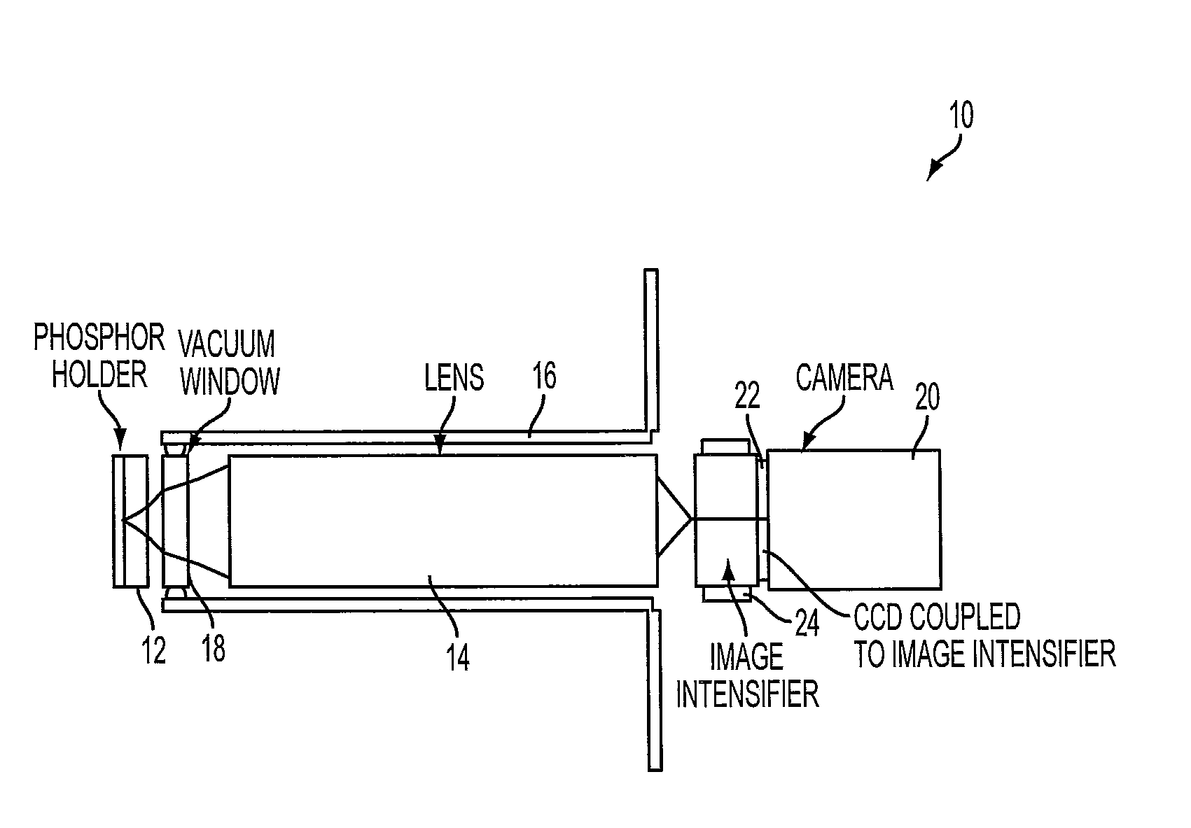
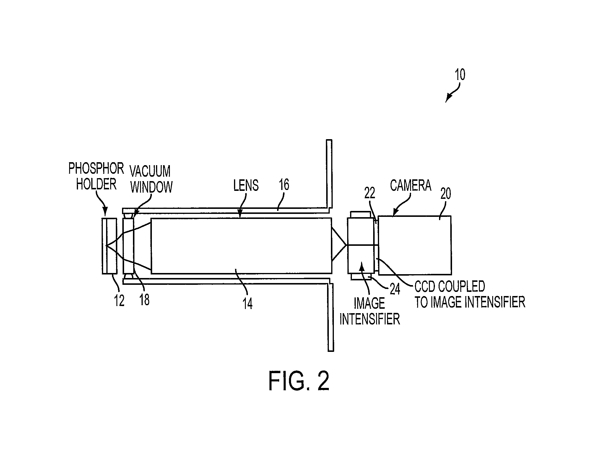
[0026]With reference to FIG. 2, a system for electron pattern imaging, denoted generally as reference numeral 10, includes: a device for converting electron patterns into visible light, such as a phosphor screen 12, provided to receive an electron backscatter...


PUM


Abstract

A system for electron pattern imaging includes: a device for converting electron patterns into visible light provided to receive an electron backscatter diffraction (EBSD) pattern from a sample and convert the EBSD pattern to a corresponding light pattern; a first optical system positioned downstream from the device for converting electron patterns into visible light for focusing the light pattern produced by the device for converting electron patterns into visible light; a camera positioned downstream from the first optical system for obtaining an image of the light pattern; an image intensifier positioned between the device for converting electron patterns into visible light and the camera for amplifying the light pattern produced by the device for converting electron patterns into visible light; and a device positioned within the system for protecting the image intensifier from harmful light.

Description

CROSS REFERENCE TO RELATED APPLICATIONS[0001]This application claims the benefit of U.S. Provisional Patent Application No. 61 / 663,102 entitled “Method and Apparatus for Electron Pattern Imaging” filed Jun. 22, 2012, which is hereby incorporated by reference in its entirety.BACKGROUND OF THE INVENTION[0002]1. Field of the Invention[0003]The present invention is generally directed to a method and apparatus for electron pattern imaging and, more specifically, to the use of an image intensifier to amplify light in an electron backscatter diffraction (EBSD) pattern collection system in a scanning electron microscope (SEM) environment.[0004]2. Description of Related Art[0005]In the field of material microanalysis, EBSD is used to study the microcrystalline characteristics of materials. The method uses the electron beam of an SEM incident on a sample and an electron imaging system to collect the electron diffraction pattern.[0006]With reference to FIG. 1, an example of a current arrangeme...

Claims


Application Information

Patent Timeline
IPC IPC(8): H01J37/244
CPCH01J37/244H01J2237/2445H01J2237/2446H01J2237/24475
Inventor BUCHHOLD, REINHARDHAMMELL, BRENTNICOLOSI, JOSEPH A.DE KLOE, PETER ANTONIE
Owner EDAX
Why Eureka
Try Eureka