Inspecting device and inspecting method

a technology of photo-emitting devices and inspection methods, which is applied in the testing of individual semiconductor devices, photovoltaic monitoring, instruments, etc., can solve the problems of inability to detect the disappearance process of the photo-excited carrier in the depletion layer of the photo-emitting device, the feeble electronescent light emitted from the photo-emitting device, and the possibility of semiconductor damage or contamination in a minute or two. , to achieve the effect of short tim

Active Publication Date: 2014-01-02
DAINIPPON SCREEN MTG CO LTD +1
View PDF8 Cites 6 Cited by
  • Summary
  • Abstract
  • Description
  • Claims
  • Application Information

AI Technical Summary

Benefits of technology

[0017]When a wide range in the photo device is to be inspecte

Problems solved by technology

In the case of the inspecting method described in the Patent Literature 1, however, the electroluminescent light emitted from the photo device is feeble.
For this reason, it is very hard to detect the process for disappearance of the photoexcited carrier in the depletion

Method used


Image

  • Inspecting device and inspecting method
  • Inspecting device and inspecting method
  • Inspecting device and inspecting method

Examples


Embodiment Construction

[0037]Preferred embodiments according to the present invention will be described below with reference to the accompanying drawings. The following preferred embodiments are specifically illustrative as the present invention and do not restrict the technical scope of the present invention. In FIG. 1 and subsequent drawings, for easy understanding, dimensions or numbers of respective parts are exaggerated or simplified and shown as necessary in some cases.

1. First Preferred Embodiment

[0038]

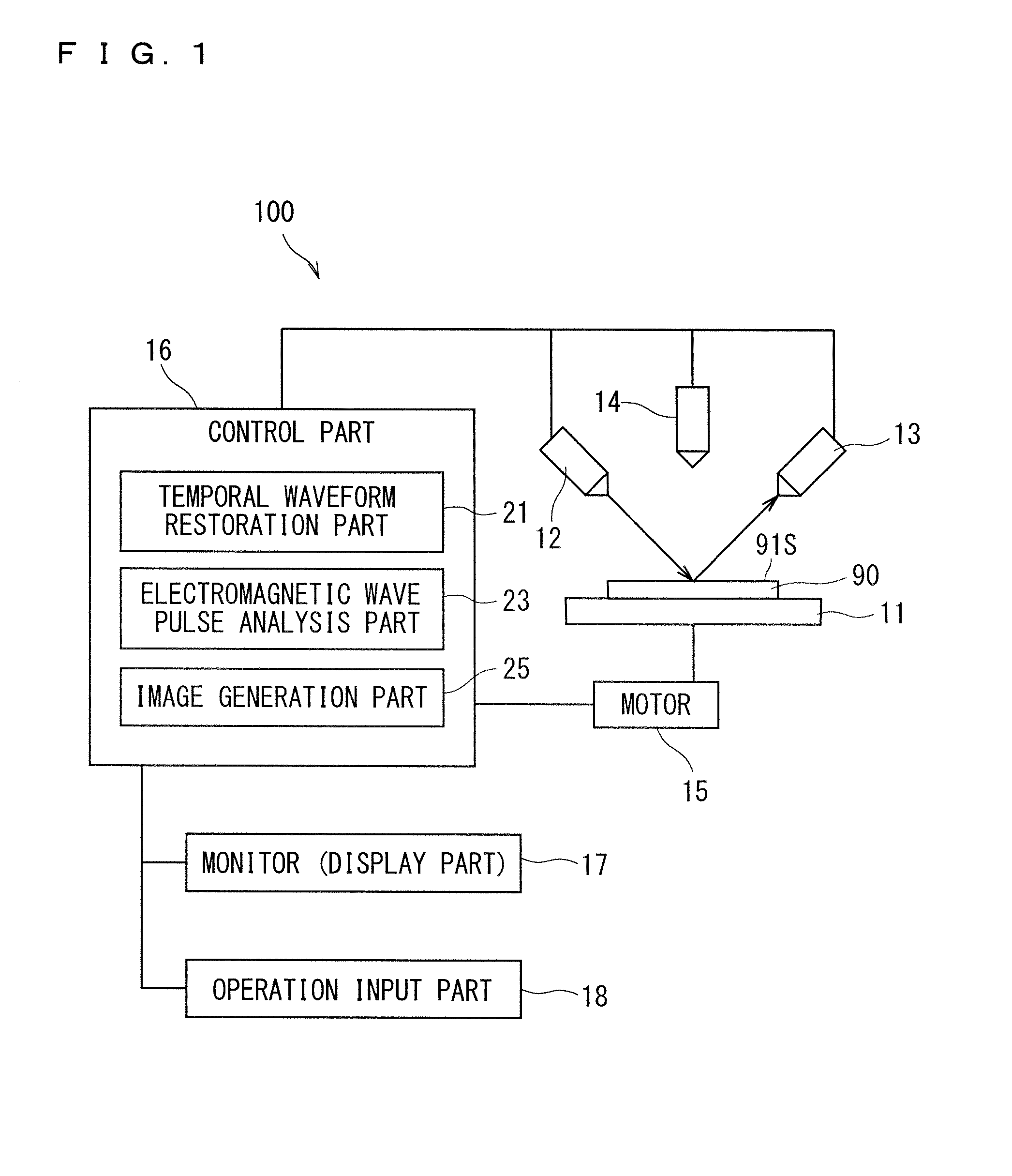
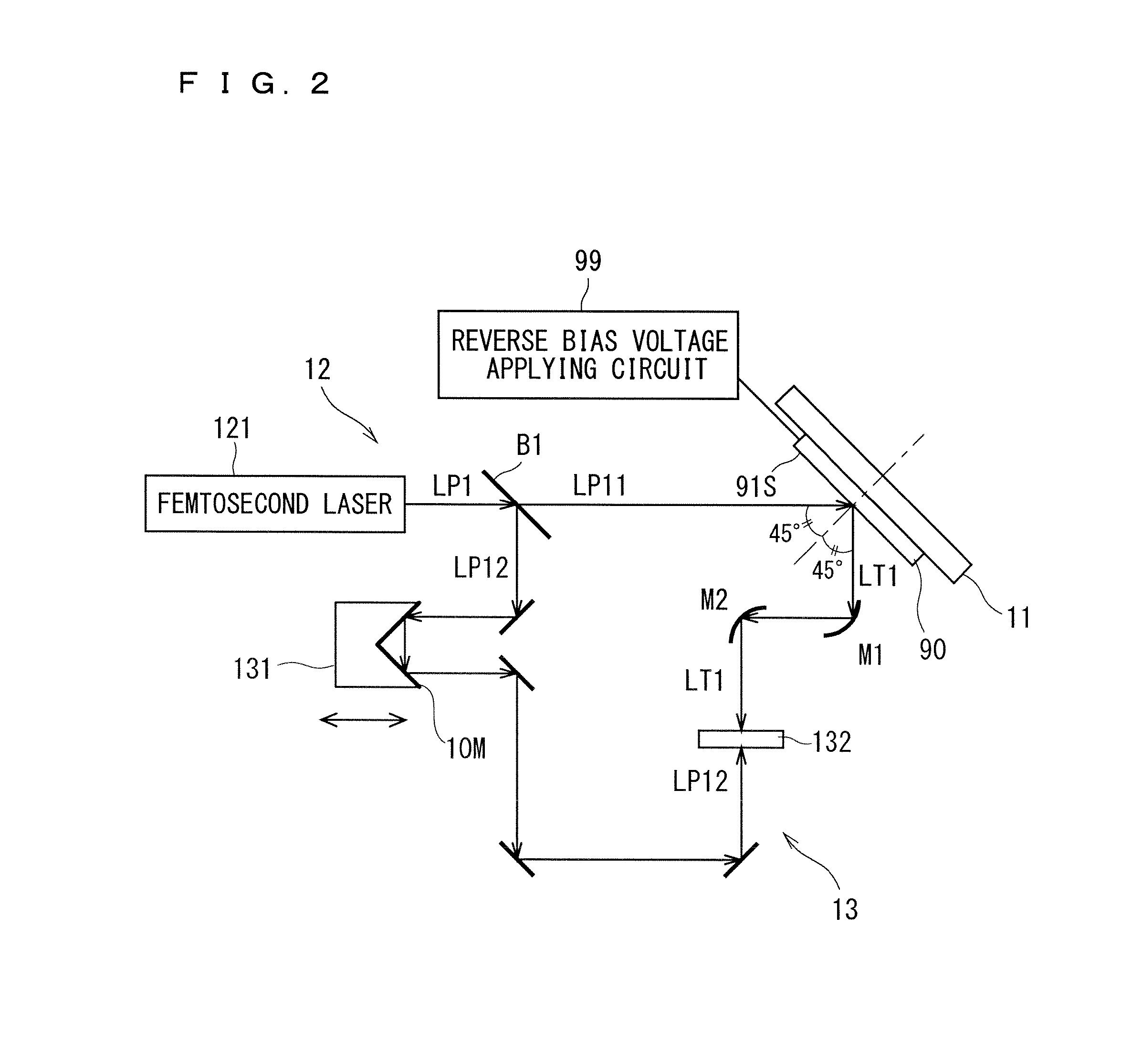
[0039]FIG. 1 is a diagram showing a schematic structure of an inspecting device 100 according to a first preferred embodiment. Moreover, FIG. 2 is a diagram showing schematic structures of an irradiation part 12 and a detection part 13 illustrated in FIG. 1. The inspecting device 100 has a suitable structure for inspecting a characteristic of a depletion layer of a solar cell 90 to be a kind of a substrate on which a photo device is formed.

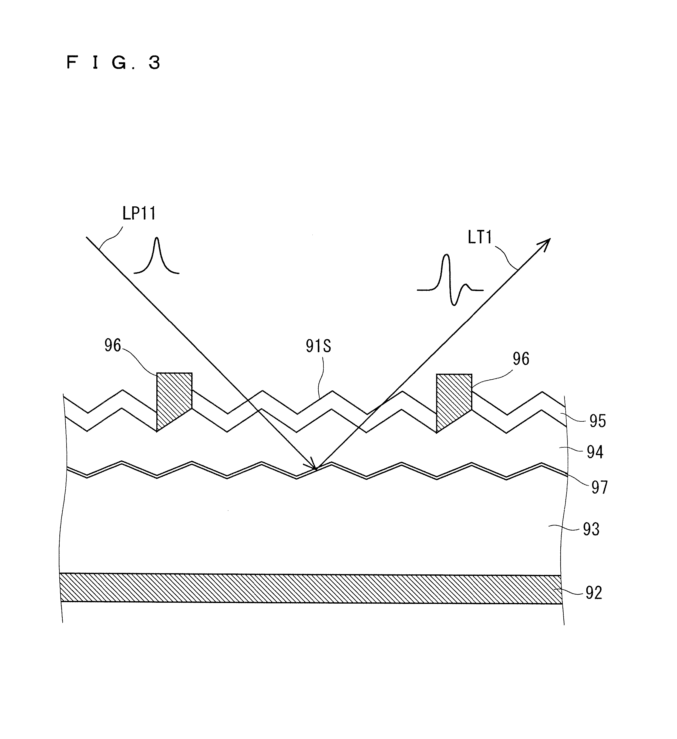
[0040]The photo device such as a solar cell has a pn junction...


PUM


Abstract

An inspecting device serves to inspect a solar cell. The inspecting device includes an irradiation part for irradiating with pulsed light and a detection part having a detector for detecting an electromagnetic wave pulse radiated from the solar cell depending on the irradiation with the pulsed light. The detector detects an electric field intensity of the electromagnetic wave pulse depending on irradiation with probe light emitted from a light source (a femtosecond laser) of the pulsed light. Moreover, the inspecting device includes a delay part for delaying a timing for detecting the electromagnetic wave pulse in the detector. Furthermore, the inspecting device includes an electromagnetic wave pulse analysis part for detecting a negative peak of the electric field intensity in a temporal waveform of the electromagnetic wave pulse.

Description

BACKGROUND OF THE INVENTION[0001]1. Field of the Invention[0002]The present invention relates to a technique for inspecting a photo device.[0003]2. Description of the Background Art[0004]A photo device utilizes photovoltaic effect, and a photodiode, an image sensor, a solar cell and the like are manufactured as products, for example.[0005]For example, solar cells utilizing single crystal silicon and polycrystal silicon occupy a mainstream, and studies are being conducted in order to enhance power generation efficiency. Moreover, the image sensor is being studied in order to increase sensitivity, to enhance an S / N ratio and to reduce a price with a focus on the security field or the sensing field.[0006]The photo device is an element utilizing photoexcited carriers (a free electron and a free hole) generated by irradiating a depletion layer of a PN junction body with light. By analyzing a situation in which the photoexcited carriers are generated in the depletion layer of the photo de...

Claims


Application Information

Patent Timeline
IPC IPC(8): G01R31/26
CPCG01R31/2605G01N21/3586G01N21/9501G01N21/956H02S50/10Y02E10/50G01R31/2607
Inventor NAKANISHI, HIDETOSHIITO, AKIRATONOUCHI, MASAYOSHIKAWAYAMA, IWAO
Owner DAINIPPON SCREEN MTG CO LTD
Why Eureka
Try Eureka