Method for manufacturing a polysilicon ingot

Inactive Publication Date: 2014-01-09
MOTECH INDUSTRIES
View PDF5 Cites 2 Cited by
  • Summary
  • Abstract
  • Description
  • Claims
  • Application Information

AI Technical Summary

Benefits of technology

[0012](e) reducing the temperature of the m

Problems solved by technology

However, by simply cooling and condensing the molten silicon, the crystal properties of the resulting silicon ingot can hardly be controlled in an effective manner.
The silicon ingot thus produced typically suffers from the pro

Method used


Image

  • Method for manufacturing a polysilicon ingot
  • Method for manufacturing a polysilicon ingot
  • Method for manufacturing a polysilicon ingot

Examples


Example

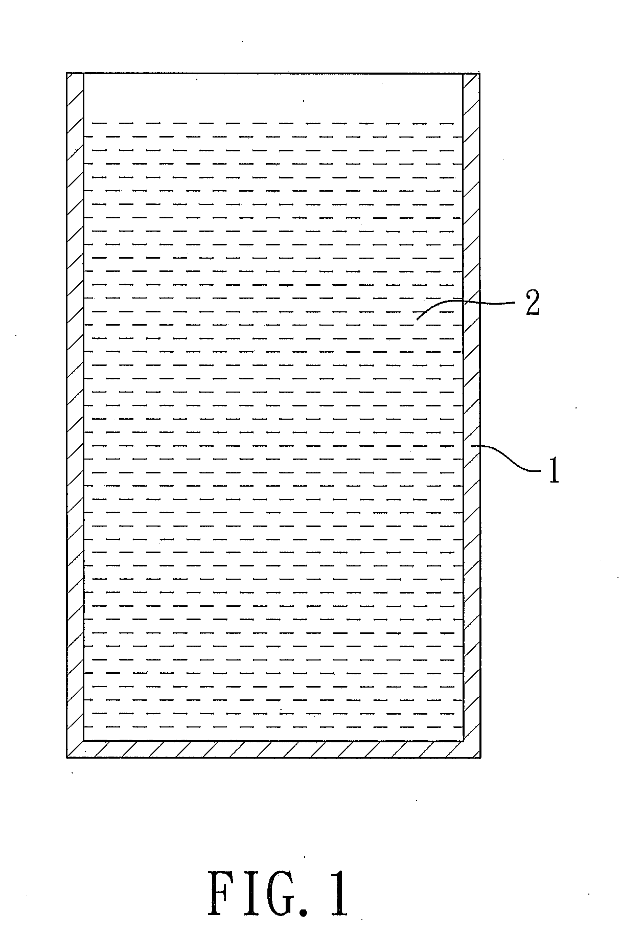
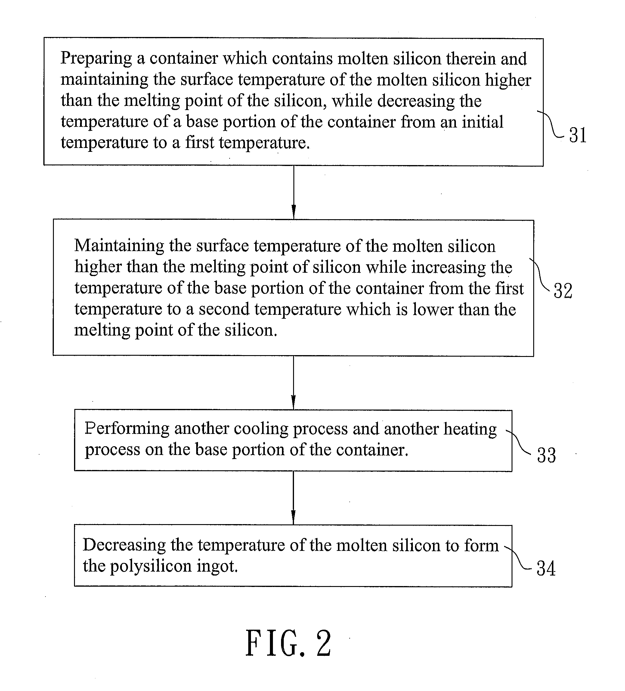
[0019]FIGS. 1, 2 and 3 show the preferred embodiment of a method for manufacturing a polysilicon ingot according to the present invention, which includes the following steps:

[0020](1) Step 31: Preparing a container 1 which contains molten silicon 2 therein. A surface temperature of the molten silicon 2 is maintained to be higher than the melting point of the silicon, while the temperature of a base portion of. the container 1 is decreased from an initial temperature (T0) to a first temperature (T1) lower than the melting point of the silicon. In this step, the molten silicon 2 in the vicinity of the base portion 11 of the container 1 undergoes a first rapid cooling process which is the so-called super-cooling step, through which silicon with a twins-crystalline structure is grown. Densely distributed twins-crystalline structures will facilitate growing of a dendrite structure, which, in turn, results in a polysilicon ingot with larger grains and a better crystal quality.

[0021]Specif...


PUM

PropertyMeasurementUnit
Temperatureaaaaaaaaaa
Timeaaaaaaaaaa

Abstract

A method for manufacturing a polysilicon ingot includes: (a) providing molten silicon in a container; (b) maintaining a surface temperature of the molten silicon higher than its melting point while decreasing the temperature of a base portion of the container to a temperature (T1) lower than the melting point at a rate of at least 2.6° C./min; (c) increasing the temperature of the base portion to a temperature (T2) lower than the melting point; (d) maintaining the surface temperature of the molten silicon higher than the melting point while decreasing and then increasing the temperature of the base portion to a temperature lower than the melting point of silicon; and (e) reducing the temperature of the molten silicon to form the polysilicon ingot.

Description

BACKGROUND OF THE INVENTION[0001]1. Field of the Invention[0002]This invention relates to a method for manufacturing a silicon ingot, more particularly to a method for manufacturing a polysilicon ingot.[0003]2. Description of the Related Art[0004]A Polysilicon wafer applied in a conventional polysilicon solar cell are typically formed by cutting a polysilicon ingot. The manufacture of the polysilicon ingot is carried out by heating a silicon material in a crucible to obtain molten silicon, which is then cooled down and allowed to condense so as to form the polysilicon ingot.[0005]However, by simply cooling and condensing the molten silicon, the crystal properties of the resulting silicon ingot can hardly be controlled in an effective manner. The silicon ingot thus produced typically suffers from the problems of having small crystal grains and lots of grain boundaries. A solar cell comprising a silicon wafer cut from the aforementioned silicon ingot will have low open circuit voltage...

Claims


Application Information

Patent Timeline
IPC IPC(8): C01B33/021
CPCC01B33/021C30B11/003C30B29/06
Inventor HO, KAI-ANCHOU, CHIEN-KANG
Owner MOTECH INDUSTRIES
Why Eureka
Try Eureka