
Semiconductor device and method of fabricating the same

a technology of semiconductor devices and semiconductor devices, applied in the direction of semiconductor devices, electrical devices, transistors, etc., can solve the problems of gcr to improve the performance of flash memory cells, and achieve the effects of reducing the operation voltage of semiconductor devices, improving the overlapped area, and improving the performance of semiconductor devices

Active Publication Date: 2014-01-16
UNITED MICROELECTRONICS CORP
View PDF13 Cites 14 Cited by
  • Summary
  • Abstract
  • Description
  • Claims
  • Application Information

AI Technical Summary

Benefits of technology

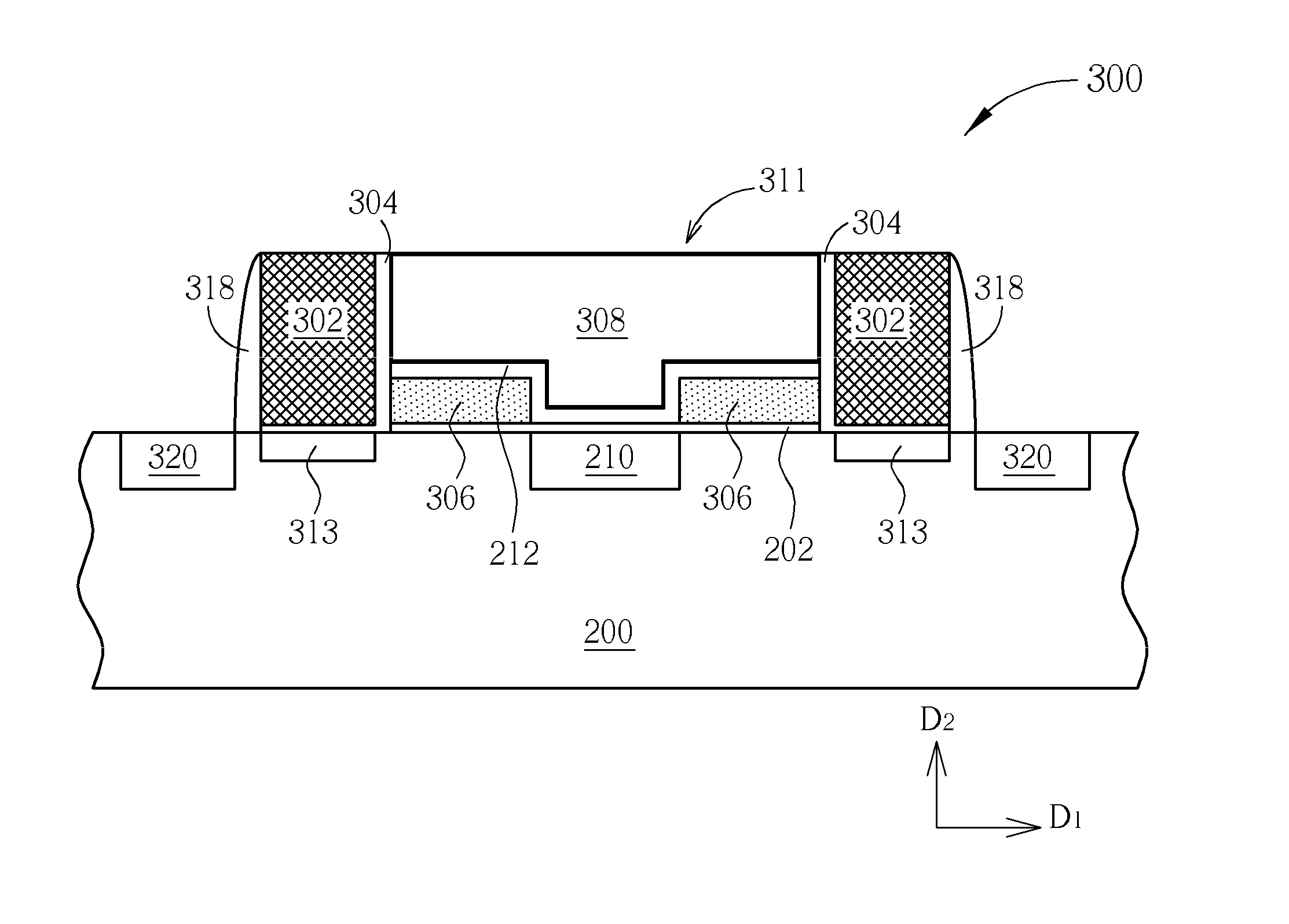
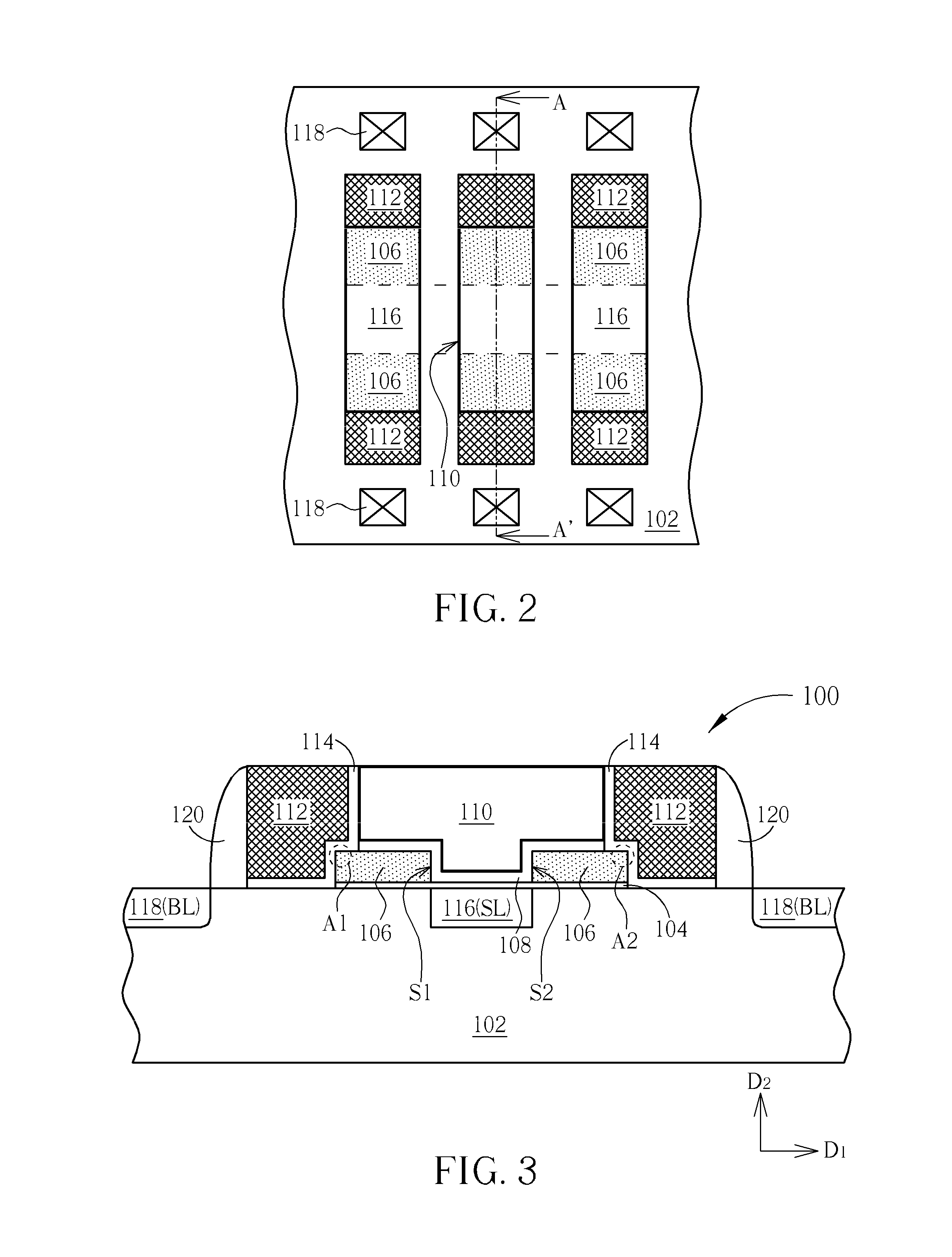
The present invention provides a semiconductor device with a high gate coupling ratio (GCR) and a method of fabricating the same to improve device performance. By using a T-shaped control gate that overlaps both the top and sidewall of each floating gate, the semiconductor device has increased GCR, reducing the operation voltage and improving performance. The first dielectric layer is conformally disposed between each floating gate and control gate, ensuring stable capacitance. These features lead to a reduced interval between the gates, resulting in better operational performance.

Problems solved by technology

Consequently, how to improve the GCR to improve the performances of the flash memory cell is still an important issue in the field

Method used


Image

  • Semiconductor device and method of fabricating the same
  • Semiconductor device and method of fabricating the same
  • Semiconductor device and method of fabricating the same

Examples


Embodiment Construction

[0016]To provide a better understanding of the present invention, preferred exemplary embodiments will be described in detail. The preferred exemplary embodiments of the present invention are illustrated in the accompanying drawings with numbered elements.

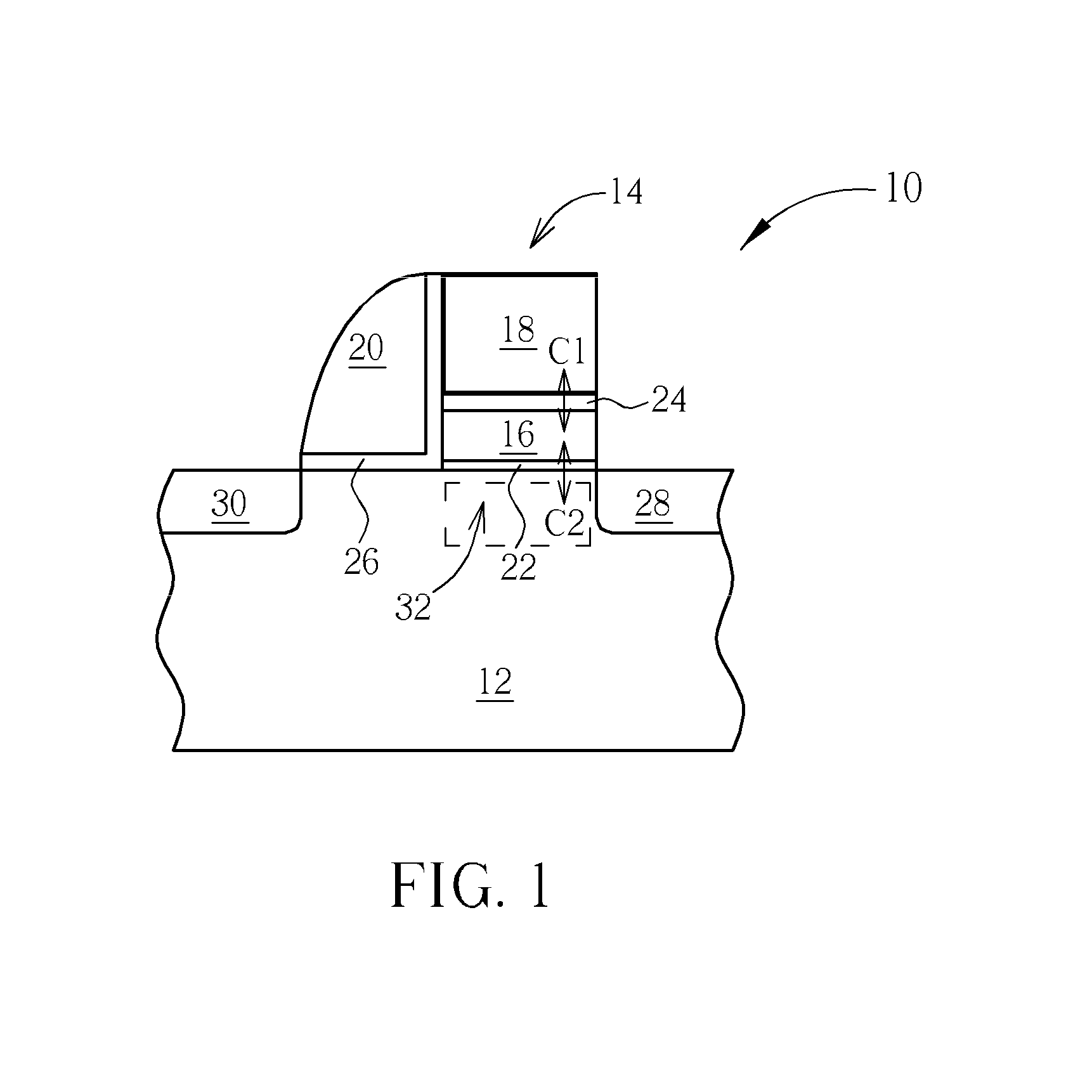
[0017]Please refer to FIG. 1, which is a cross-sectional diagram illustrating a semiconductor device according to an exemplary embodiment of the present invention. As shown in FIG. 1, a semiconductor device 10, such as a flash memory cell, includes a semiconductor substrate 12, a gate stack 14 disposed on the semiconductor substrate 12, and a select gate 20 disposed at a side of the gate stack 14. The gate stack 14 includes a floating gate 16 and a control gate 18. The semiconductor substrate 12 may include a substrate composed of Si, AsGa, silicon on insulator (SOI) layer, epitaxial layer, SiGe layer or other semiconductor materials. The floating gate 16, the control gate 18 and the select gate 20 are commonly made of polysilicon,...


PUM


Abstract

A semiconductor device includes two floating gates, a control gate and a first dielectric layer. The floating gates are disposed on a semiconductor substrate. The control gate partially overlaps each of the floating gates, and a part of the control gate is disposed between the two floating gates. Furthermore, the first dielectric layer disposed between the two floating gates and the control gate has a fixed thickness.

Description

BACKGROUND OF THE INVENTION[0001]1. Field of the Invention[0002]The present invention relates to a semiconductor device and a method of fabricating the same, and more particularly to a semiconductor device having a high gate coupling ratio (GCR) and a method of fabricating the same.[0003]2. Description of the Prior Art[0004]A flash memory is a non-volatile memory, which can preserve data within the memory even when an external power supply is off. Recently, because the flash memories are re-writable and re-erasable, they has been widely applied in the fabrication of electrical products, such as mobile phones, digital cameras, video players, personal digital assistants (PDA) or systems on a chip (SOC).[0005]With the trend of miniaturization of the electronic products, the smaller size of the flash memory cell 10 reduces the gate coupling ratio (GCR). Consequently, how to improve the GCR to improve the performances of the flash memory cell is still an important issue in the fieldSUMMA...

Claims


Application Information

Patent Timeline
Patent Type & Authority Applications(United States)
IPC IPC(8): H01L29/788H01L21/336H10B69/00
CPCH01L29/42324H01L29/7881H01L29/7882H01L29/40114H01L29/66825H10B41/30H01L21/266H01L29/42328H01L29/42332H01L29/6653H01L29/6656
Inventor HSU, CHENG-YUANREN, CHIWEN, TZENG-FEI
Owner UNITED MICROELECTRONICS CORP
Learn More